Sunday, 9 June 2024

MOS 6550 RAM Chips - An interesting (if flawed) idea

This is the MOS MPS 6550, a 1K x 4 static RAM chip.

It seems like a normal static RAM chip as you would expect in the late 1970s.

However, as you can see it is different to other chips.

Don't worry, I am not going to do the "I know my place" class / status joke again.

Comparing it to a 2114 and a 6116, you can see it is not the normal 300mil narrow DIP package, or the standard 600mil DIP package. It is 22 pin 400mil spacing. I don't think I have seen another 22pin chip, or one with 400mil spacing (other than a Sony CCD chip).

The other way it is unusual is that it has 4 chip select lines. CS1 and CS2 have to be high, and /CS3 and /CS4 have to be low to enable the chip. What is the point of that you might ask? well, it can simplify address decoding.

The actual selection is triggered by the PHI2 clock input, with nothing happening until the clock is high.

Take for example the Commodore PET 2001. This had 18 of them. 16 to give 8K x 8main RAM, and another two as 1K x 8 video RAM (giving 1024 characters, 25 rows of 40 characters with a few to spare). Someone has clearly had fun marking the failed ones on this board.

I think this was the first and last use of the 6550 chip, and indeed by the end of the life of the PET 2001, even that had switched to more normal 2114 RAM chips.

For simplicity, I have only shown the 4K version, and have bussed most of the signals which are wired in parallel. These are 4 bit chips (like the 2114), so a pair of chips is required for 1K, with D0-D3 wired to one chip, and D4-D7 to the other.

The PET has its memory split into sixteen 4K blocks, and a 74154 4 to 16 line decoder is used to decode A12-A15 to generate sixteen block select lines. Here /SEL0 is used, which is low when addresses in the range 0000-0FFF are accessed. (/SEL1 is 1000-1FFF, /SEL2 is 2000-2FFF and so on up to /SELF as F000-FFFF)

Starting on the left with J4, this needs to be placed in RAM at 0C00-0FFF. The top byte of the address is 0000 11xx. A15 to A12 are handled by the /SEL0 line and A0 to A9 are handled by the 6550 RAM chip, so it is only A10 and A11 which need to be decoded. In this case, both are high.

You're got four enable lines, so BA10 and BA11 need to be high, and /SEL0 needs to be low. The spare one is just connected to 0V. OK, that works.

J3 is 0800-0BFF, the top bits are 0000 10xx, so BA11 is high, and BA10 is low. /SEL0 again is low, and the spare CS1 is tied to 5V.

No problem, the 6550 has got that covered.

J2 is 0400-07FF, 0000 01xx, so BA11 is low, and BA10 is high. /SEL0 again is low, and the spare CS1 is tied to 5V.

Hey this is easy.

Finally J1 covers 0000-03FF, 0000 00xx. So BA10 and BA11 and /SEL0 are low. Ah, oh dear. We don't have enough inputs. We need three active low inputs and we have only two.

To get around that, they created a /BA11, an inverted version of BA11, so all is good, but is that cheating? 

That was J1-4, which are wired to D4-D7. The other 4 bits were provided by I1-4.

All of the decoding here is identical, and all the other lines are wired in parallel apart from the four data pins, which are connected instead to D0-3.

There was a planned base model PET 2001-4, with only 4K, but I don't think that was ever released.

I think they were all sold as PET 2001-8 with 8K.

Another 8 chips wired identically, other than all the /SEL0 lines were instead connected to /SEL1 and covered the address range 1000-1FFF.

So is this a good idea? I guess it saved some external decoding logic. Maybe.

The great thing about 6550 RAM is they had multiple chip select lines so they could effectively be wired in parallel without additional decoding logic.

The awful thing about 6550 RAM is they had multiple chip select lines so they could effectively be wired in parallel without additional decoding logic.

This decoding turned out to be an Achilles heel, and seemed to fail in a way that left the RAM enabled when it shouldn't have been.

The result is multiple chips being enabled at the same time, all trying to write to the bus at the same time.

Bus conflict.

Heat.

A war of attrition.

The chips with the beefiest transistors wins out in the end. If you have 6550 RAM chips (or indeed 6540 ROMs) that are getting very hot. They don't just need a heatsink, they needs to be removed, as they slowly destroy more and more of the working ones.

The main RAM can be replaced with a PET ROM/RAM and the video RAM with a 6550 Video RAM replacement board (see end of the post for links).

Towards the end of the production life of the PET 2001, they changed to using 2114 SRAM and standard mask ROMs, and I don't think the 6540s or 6550s were seen again anywhere else.

There is a schematic set for a PET 2001 with 2114 RAM and mask ROMs, but I have never actually seen one. Only the 6550/6540 and 2114/6540 versions.

As we saw earlier, the 2114 is a smaller chip, 18 pin and 300mil wide. It has only one /CS line, and no need for the clock signal.

It is interesting to look at the changes they made to the PET 2001 to use 2114 RAM chips instead of 6550s. 

How much extra decoding logic did they actually need?

With only one /CS line, they had to use some additional decoding to select the RAM chips.

This is the whole 8K RAM composed of 8 pairs of 2114 chips, and it is still pretty minimal.

All they added was a single 74LS139 dual 2 to 4 line decoder. And as they no longer needed the /BA11 signal, they would save a gate elsewhere, so not a major difference in the end.

I say 2114s, although one board I had in for repair had TMS4045 chips instead, but they are compatible.

I have seen others with actual 2114 chips, although this one was quite a pick and mix of makes and part numbers.

The RS and the Tesla (not that one) chips were presumably later repairs, with the soldered ones being factory fit and still a mix of types.

One of the factory fitted ones shows they even got MOS to make 2114 chips, so they still kept the in-house savings.

I think they had some good ideas with the decoding, but maybe would have been better to have maybe gone for a 28 pin package and added the other 4 data lines, making it a byte wide. They would still have 2 extra pins, maybe extra /CS lines to avoid needed /BA11 or extra address lines to make a 2K or 4K chip.

Or go for a more standard 24 pin and lose chip select lines and still be able to go byte wide and 2K.

Oh wait, that's a 6116.

Why didn't they make a 6116 then you would only need 4 of them for an 8K PET and could have left space for 16K or even 32K.

(they were around a few years later for the VIC20 CR and the ZX81 / TS1000, maybe earlier, but maybe they didn't have the silicon wafer size to do it? or yield problems?)

And a 62256, 32K on a single 28 pin chip would have been even better, but they were several years away from those. This is the RAM arrangement on the Mini PET.

One chip, decoded on A15 being low (0000-7FFF) for the maximum 32K RAM.

It is interesting to note that they did not move to larger static RAMs on later boards. They went to dynamic RAM, 8 or 16 4116 chips, giving 16K or 32K. They must have been significantly cheaper as their use required a change to the transformer to add an extra winding, and the appropriate components to make the additional +12V and -5V supplies required by these chips. Plus a page of schematics worth of extra parts to handle DRAM refresh.


Advertisements

I have an assortment of PET repair parts available from my SellMyRetro store, many of which are shown here.

6550 Video RAM Replacement

2114 Video RAM Replacement

6540-101 Character ROM Replacement

PET Video Out

PET Diagnostics

PET IEEE-488 Diagnostics

PET 2001 Video Glitch Fix

PET ROM/RAM

SD2PET Power Tap

Dual 9 way D Userport Joystick

Or if you would rather a whole PET made from modern parts, the full range of Minstrel and Mini PET kits and accessories are available form my SellMyRetro store.

Everything can be found here:

Patreon

You can support me via Patreon, and get access to advance previews of posts like this and behind the scenes updates. These are often in more detail than I can fit in here, and some of these posts contain bits from several Patreon posts (they also got an extra post covering the history of my 6550 video RAM board). This also includes access to my Patreon only Discord server for even more regular updates.

Sunday, 2 June 2024

Building a divIDE Spectrum IDE interface

As part of something I was working on, I was looking into the ZX Spectrum divIDE, quite an old project, but a way of getting a disk interface for the Spectrum before the days of the divMMC.

The project this was for will probably not happen now (#Z80RIP) but I would still like to get this working.

I remembered seeing an all through hole version, and indeed I thought I had one at one point, but I couldn't find it. (Ed: I now remember it came in with a ZX Spectrum repair a long time ago and went back to the owner with the repaired Spectrum)

So, I had a look around for built units or kits, but all I found was someone selling bare PCBs on ebay. The divIDE 5.7C seemed to be the version everyone was using, so I ordered one of those.

I wasn't too impressed with the PCB. Just personal preference, but I don't like the way the PCB was marked out, quite difficult to follow. It may be ebay seller was just using a random set of gerber files they found online?

How on earth are you meant to work out what goes where?

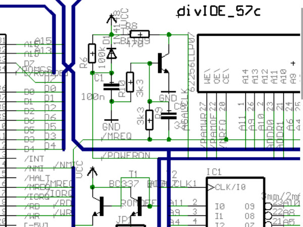
Luckily, there is a schematic........

Oh dear, that's even worse.

All of the versions online seem to be variations of that. Some in colour, some not.

I finally found a better one thanks to Nightfall Crew.

Comparing that to what I could read from the PCB and the schematic it seemed right, and various photos online show built units with two missing parts (C8 and RN1) not fitted.

The only issue I had with parts was the BF199 transistor. I didn't have one of those and couldn't see any in stock at my usual suppliers. I instead used a BC548 which had similar (but slightly better) specs, but unfortunately a different pinout.

Fingers (and legs) crossed this minor bodge will work.

Looks fine, you would likely not spot it if you were not looking for it.

All populated and ready to go.

There is a 28C64B EEPROM on the board which needs to be programmed with the appropriate firmware using a program on the Spectrum.

You load up the program, then remove jumper JP2 (which is marked behind the jumper where you can't see it)

Lots of flashing bright colours as usual, seems to be going well.

And there it is flashed.

So I switch off, refit JP2 and turn the power back on but I don't get a boot screen, all I get is a copyright Sinclair screen?

OK, let's try that again.

No, same.

Hmm, there should have been a boot screen just like the divMMC.

Speaking of which, just to check, I tried going through the same process with a divMMC future, and that worked correctly.

I also tried FATware, an older firmware which should support the same hardware, that appeared to program correctly, but again did not work. I later retried it and at least got an error this time. Not sure what it means though.

I grabbed another Spectrum from the pile, in case the problem was with the two Spectrums I had been testing with. I was pretty sure it wasn't, since the divMMC worked, so I don't think it was a bad M1 line for example.

Trust me to pick one I hadn't updated.

Just needed a quick composite mod and a switching regulator replacement.

Lets retest with that.

Did it make a difference? No.

OK, lets' reprogram the GALs, and lets's also try a set of Atmel ATF22V10C as well as the Lattice 22V10B.

No, that hasn't helped.

OK, maybe my substitute transistor is not suitable?

I had to turn to ebay again I am afraid, but I got a pack of BF199s.

Being the correct part, that could be installed without the need for the twisted legs this time.

Did that fix it? No.

I have revisited this a few more times, trying different EEPROM and GAL chips and trying to program the EEPROM directly, but not getting anywhere.

I don't know what is going on there. It is possibly my build is bad, but I have checked over all the solder joints etc. and I can't see anything.

It is possible the PCB is bad, given the silkscreen mess, it is possible there are also errors with the traces.

It is possible I have the wrong GAL files, or my GALs are all bad, or my programmer is somehow not programming them correctly. (although I use the same chips and the same programmer for other things.)

Anyone got any ideas?

Anyone had any success building this version of the PCB recently?

Anyone got a working version of this I could borrow and compare?


Advertisements

The full range of Minstrel and Mini PET kits and accessories are available form my SellMyRetro store.

All the links can be found here:

Patreon

You can support me via Patreon, and get access to advance previews of posts like this and behind the scenes updates. These are often in more detail than I can fit in here, and some of these posts contain bits from several Patreon posts. This also includes access to my Patreon only Discord server for even more regular updates.

Sunday, 26 May 2024

The actual Kempston joystick interface is not the best Kempston compatible joystick interface

I know I have several of these, but I couldn't find any when I was working on the previous post where I looked into Kempston compatible joystick interfaces  - http://blog.tynemouthsoftware.co.uk/2024/05/minstrel-joystick.html

I have now found an actual Kempston joystick interface.

Turns out Kempston Micro Electronics were actually based in Kempston, Bedford, UK.

All the best hardware comes from companies named after their location.....

This is a two chip design. Both slightly unusual choices.

Problem 1

The one on the right is a 4071 CMOS quad OR gate, why not use a 74LS32? Maybe they were cheaper, or they liked the slightly different pinout? (the outputs are all on the middle pins 3,4,10 and 11).

CMOS and TTL do not usually mix, but you can generally drive TTL inputs from CMOS outputs, just not the other way around. The inputs are all direct from the NMOS / CMOS Z80, so it should be OK, but it does no seem ideal.

The chip on the left is a 74LS541, also unusual. Like many of the 500 series, this is a version of another chip with an alternate pinout, in this case a 74LS241. The 500 series often all the inputs on one side, all the outputs on the other, to make PCB layout neater, I like the 573 and 574 for that.

I will give them credit, the layout is indeed very neat. All single sided, with no jumper links.

Problem 2

The decoding is a little lacking. They have used A5, A6, A7 and /IORQ all low, which responds to an IO request over the address range of 00-1F (0-31). However as well as the read requests it needs to respond to, it will also respond to writes and interrupt acknowledge signals. This could cause a bus conflict as both the Z80 and the 541 buffer will be writing to the databus, so is not ideal. They had a spare OR gate, so they could have added /RD low as an extra condition to fix that.

Problem 3

Also unusual is the way the 9 way D joystick port is wired. The common on the joystick port, pin 8, is connected via a 4.7KΩ resistor to 5V, and the autofire power, pin 7 is not connected.

This interface is (by definition) Kempston compatible, so follows the standard protocol of a byte read from address $1F / 31, with the bits set as 0 normally and 1 when active.

To achieve that, with the non-inverting buffer chip they have selected, all the pins are pulled low with 10KΩ resistors, including the three unused bits. The switches in the joystick are used to switch to 5V (via the 4.7KΩ resistor). These signals are then passed though the non-inverting buffer when the port is read.

That arrangement isn't really Atari / Commodore compatible, because the common pin 8 is normally connected to 0V and pin 7 supplies 5V for autofire circuits etc.

Pin
Kempston
Atari / Commodore
1
Up
Up
2
Down
Down
3
Left
Left
4
Right
Right
5
-
- / Paddle / Fire 3
6
Fire
Fire
7
-
5V
8
5V
0V
9
-
- / Paddle / Fire 2

That means most (if not all) autofire circuits will not work. Some will do nothing, others may do odd things like fire continuously, or fire when moved in any direction. Some may even be damaged by the reverse polarity.

What's that you say? you want a blog post with a deep dive into autofire circuits? One day maybe.

Problem 4

Having the common wired directly to 0V would mean you should get pretty much 0V at the input of the logic gates. Any resistance due to the switch contacts, cables and connectors should be insignificant in relation to the pullup resistors that are typically 10KΩ.

In a worst case, with a really poor cable and bad contacts you might get 100Ω combined resistance. With a 10KΩ pullup, that would still give an output of 0.05V, and in practice, it is likely to be only a few ohms, so only a few mV above 0V.

Kempston have fitted a 4.7KΩ current limiting resistor in the common line. The value of this is quite close to the 10KΩ pull downs resistors. This will form a potential divider and the voltage input to the buffer chip will not be 5V when you hit fire or move the joystick. Normally you would plan them to be orders of magnitude apart so the potential divider impact would be insignificant.

With just fire pressed or a movement in a single direction, the potential divider created by the 4.7KΩ resistor and a single 10KΩ pulldown will give about 3.4V. Not 5V as would be ideal, but well in the range of logic 1 for a TTL chip (which should be anything over 2.0V).

With fire pressed at the same time as moving in a direction, or a diagonal movement which will register as two directions at the same time, there will be two 10KΩ pull downs in parallel.

I have redrawn that with the switches removed and replaced by shorts or gaps, so you can see the resistors that are still in circuit and the the ones that are not.

This means the potential divider is now 4.7KΩ and 5K, so the output voltage would be about 2.6V. Again not ideal, but still just about within range.

In the (admitedly rare) case of fire and a diagonal at the same time, would be three 10KΩs in parallel. That would make their combined resistance 3.3KΩ, giving an output voltage or around 2.1V, very close to the 2.0V threshold. If the 5V line dropped only slightly to 4.8V, the input to the logic gate would drop below 2.0V and into the no mans land between logic 0 and logic 1, so it may not always read correctly if you press fire when moving diagonally.

Could they have done it differently?

I am not sure why they decided to deviate from the standard established by Atari in 1977. They could have used a 74LS540 instead of a 541. That is an inverting buffer, so they could have implemented a more standard interface with pin 8 as 0V and pin 7 as 5V, and pullups on the inputs up to 5V.

Something like this:

I have left it with a 4071, but ideally a 74LS32 would be more appropriate.

This version has no extra parts (in fact there is one fewer part as there is no need for the contentious 4.7KΩ resistor) and makes it more compatible with other 9 pin D joysticks. I guess they must have had their reasons.

I also used the spare gate to add /RD to the decoding to stop it responding to writes and interrupt acknowledges. Again, that's for free if they had chosen to, it would not add any additional propagation delay, and I think would have routed neatly without a need for a jumper link.

Actually, I've just checked and the 541 has two enable inputs which are ORed together, so both have to be low to enable the buffer. They have them both wired to the output of the OR gate address decoder, so they could have just wired one of them directly to /RD and not even needed the spare gate.

So in several ways, the Kempston joystick interface is not the best Kempston compatible joystick interface.

Problem 5

This particular example also has one more thing against it, a damaged edge connector.

I have picked up a few interfaces of various type with edge connectors that are broken like this one. The material seems to be quite brittle and the connector cracks all the way along one side. I guess someone left this connected to their Spectrum and then it got knocked.


Advertisements

My own take on a Kempston compatible joystick interface is the Minstrel Joystick.

This is available from my SellMyRetro store

This can be fitted with an edge connector and used directly on a Minstrel 2 or 3, or a ZX80, ZX81 or ZX Spectrum. Or it can be used as part of the Minstrel Expansion Bus.

Those and the full range of Minstrel and Mini PET kits and accessories are available form my SellMyRetro store.

All the links can be found here:

Patreon

You can support me via Patreon, and get access to advance previews of posts like this and behind the scenes updates. These are often in more detail than I can fit in here, and some of these posts contain bits from several Patreon posts. This also includes access to my Patreon only Discord server for even more regular updates.