The Commodore 64 has a processor with a 64K address space, and has 64K of RAM installed, so any ROMs need to be switched in and out of blocks of addresses within that space. There are various combinations available which swap in the system ROMs and the two 8K regions on the cartridge slot.
This is all controlled by the PLA chip, which is why you get big problems when they fail. (see a previous blog post on Commodore 64 cartridges for more information on the different modes)
As designed, a Commodore 64 cartridge would contain one or two 8K ROM chips, in various combinations, so you could have up to 16K of ROM code for your game or utility. There are two chip select lines ROM_L and ROM_H which are used to activate the ROM chips as required.
Due to practical issues of size and cost and sanity, they had to do that electronically. What they did was build the cartridge as if it was a single 8K ROM cartridge, so on boot a single 8K ROM is selected and works as if it were a normal cartridge. There are some IO ranges on the cartridge port, and they used one of these to add a register which latched in the address of the ROM that was required, and next time the 8K ROM range was accessed, the appropriate ROM chip would respond. No robot arms were required. The robot arms unions were furious.
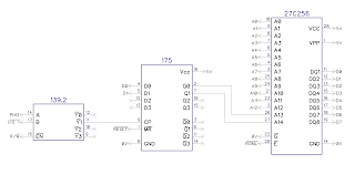
The 74LS175 is a 4 bit latch, and latches D0 and D1. This is a two bit address of the ROM. It has a reset line connected, so is reset to 00 when the C64 is reset. The right hand half of the 74LS139 is used to decode this two bit address into four select lines, one for each ROM chip, only active when the /ROM_L line from the cartridge port is low, so working like a single EPROM.
Here the right hand half of the 139 is not used, and instead the two bit address forms the upper address lines of a 32K ROM chip. This gives the same result as the four ROM chips in the previous design, but at a cost and complexity saving.
Of course, the next logical step is to connect up an extra data line to the latch, and use a 64K ROM chip, and as if by magic, you have a 64K ROM bank cartridge, selectable by writing a 3 bit address to the IO port.
At this stage, when you are implementing a practical cartridge, there are other things to consider, which add complexity to the simple schematic above. Mainly it is adding jumpers to allow different ROM chips. Borrowing the table from the previous blog post, on the Marina 64 cartridge we removed a few of the less common chips to give a 32K -1MB range with only a single jumper to select 28 pin or 32 pin ROM chips.
So there you have it, that sort of bank switching is common on larger ROM cartridge (such as those produced in the 1980s by Ocean), and on modern multicarts (such as the VIC20 Penultimate Cartridge).
A production surface mount version of the Marina 64 32K-1MB banked ROM cartridge is available from TFW8b.com.


