Sunday 23 February 2020

Commodore PET USB keyboard / Keyboard testers

There were several variations of the keyboard used on the Commodore PET, but all used the same 20 pin header with pin 2 missing as the Commodore 64 and VIC 20, although the pinout is different (and is different again from the C16 which also uses the same pin header). In order below, the chiclet keyboard, normal/graphics keyboard and business keyboard.
I originally build a USB keyboard adapter for the Commodore PET keyboards for use as a testing tool when cleaning keyboards. The early PET keyboards do occasionally get into a state where none of the keys are responding, unless maybe you press them really hard. You can start to think it is a problem with the keyboard IO chip, rather than the actual keyboard, so it is useful to be able to test the keyboard in isolation.
I wasn't planning on selling those, but I was occasionally asked to build them, and did until I ran out of boards. I was approached by someone wanting to use one of these, but for the keyboard from an 8032-SK. This is the recased 80 column, 32K RAM PET (8032) in the nice rounded not-designed-by-Porsche case, and an absolutely massive separate keyboard (SK).
The keyboard inside was the same as the business keyboard above, but in a detectable keyboard with a nice coiled lead and a 25 way D plug on the end. The same type of plug as used on the SX-64, C128 and CBM II, but of course with a different pinout.
I had only made a few PET USB keyboard adapters, so I had been using an existing board to make them, and didn't have any of those left, so wasn't planning to make any more, but when money was waved under my nose, I was persuaded to make some more.
The 8032-SK used the same board as the standard 8032 in the not-at-all-rounded case, which had the 20 pin header, and there was a cable on a bracket which adapted this to the 25 way D connector for the external connection.
I could have got some more of the old boards, and reused the adapter cable, but I thought I may as well do this properly.
There is now a 25 way D socket onboard, so the SK keyboard plugs in directly to one side, and the USB cable to the other.
I designed the new board to replace that bracket and pick up on the same mounting holes.
That all fits in very nicely. Job done.
You might have noticed a row of holes on this board. Yes, I added a footprint for the 20 pin header, so I can now make a 'universal' board for testing PET keyboards which will take one of the pin header versions or the 25 way D.
I also took the opportunity to delete the 25 way D connector and make a smaller version for just the 20 pin keyboards.
I went for jumpers to select the mapping type, so there weren't too many build options.
The chiclet keyboard on the original 2001 and the later graphics keyboard are interchangeable on the PET, and these were used on almost all of the PETs with 40 column screens, the 2000 series, 3000 series and both of the different 4000 series (don't ask).
The only reason I have different jumper settings for the graphics keyboard is some of the non-standard keys are mapped differently. The layout without numbers on the top row doesn't seem too bad on the chiclet, but seems a bit mad on the graphics keyboard.
Although the OFF/RVS key is in the same position in the matrix, it is to the left of Q on the graphics keyboard and suits being mapped as tab. On the chiclet, it is bottom left, so is mapped as the Windows key.
You can also use the chiclet mapping with my Commodore PET replacement keyboards, which are designed as a drop in replacement. (to save you visiting the FAQ, no it doesn't come with keycaps, no I don't know where you can get any, if I did, don't you think I would have used them?)
The business keyboard was used on the 8000 series of 80 column PETs (including the SK models). This has a more familiar layout, although the matrix is laid out very differently to the graphics keyboard, so any games which scan the keyboard directly do not translate between systems (even if you can get around the 40-80 column thing in hardware or software).
The business keyboard is almost, but not quite, entirely unlike the later VIC20/C64 keyboard. They do share the same mechanical frame (you can see the stickers under the unused holes where the keypad was), but the PCB is wired differently, yet another different keyboard matrix, so they two are not interchangeable.
So these are the new Commodore PET USB keyboard adapters, with a 20 pin header, a 25 way D, or both.
These are available now from my Tindie store. As ever, please use responsibly.


2023 Update

USB Keyboard Controller Kits are available from my Sell My Retro store:

Sunday 16 February 2020

How banked ROM cartridges work


Following on from last week's blog post on the new Marina 64 banked ROM cartridge for the Commodore 64, I thought I would answer a few of the questions that post raised by going into a bit more detail.
The Commodore 64 has a processor with a 64K address space, and has 64K of RAM installed, so any ROMs need to be switched in and out of blocks of addresses within that space. There are various combinations available which swap in the system ROMs and the two 8K regions on the cartridge slot.
This is all controlled by the PLA chip, which is why you get big problems when they fail. (see a previous blog post on Commodore 64 cartridges for more information on the different modes)
As designed, a Commodore 64 cartridge would contain one or two 8K ROM chips, in various combinations, so you could have up to 16K of ROM code for your game or utility. There are two chip select lines ROM_L and ROM_H which are used to activate the ROM chips as required.
What happens if you want more? Well, in the case of the Magic Desk 1 cartridge, they needed 32K, so the code would need to be on four 8K ROM chips, but the cartridge could only be 8K or 16K? I don't know exactly what happened, but my theory is they decided they could use a single 8K ROM cartridge with one of the ROM chips in, and the other three ROM chips in a little tray by the side. Each cartridge would be supplied with a robot arm and whenever they wanted something on one of the other ROM chips, the robot arm would unplug the current ROM chip and plug in one of the others.
Due to practical issues of size and cost and sanity, they had to do that electronically. What they did was build the cartridge as if it was a single 8K ROM cartridge, so on boot a single 8K ROM is selected and works as if it were a normal cartridge. There are some IO ranges on the cartridge port, and they used one of these to add a register which latched in the address of the ROM that was required, and next time the 8K ROM range was accessed, the appropriate ROM chip would respond. No robot arms were required. The robot arms unions were furious.
The 74LS139 is a dual 2 to 4 line decoder, in each half, one of four outputs goes low based on a two bit address on the input. Here, the left hand half of the 74LS139 is used to generate the clock pulse for the data latch. This is triggered on the high going edge, so the output goes low when the clock is high, I/O 1 region is low and write is low, so the first part of the write cycle. Whilst the clock is high, the databus is being prepared with the data to be written, and when the clock goes low, it should be ready, so is latched into the 74LS175. (note on the only schematic I have found, this is incorrectly shown as connected to pin 12 of the 139, but I believe this to be a mistake as it would latch too early in the cycle, so have shown the connection to pin 11 in my redrawn schematics)
The 74LS175 is a 4 bit latch, and latches D0 and D1. This is a two bit address of the ROM. It has a reset line connected, so is reset to 00 when the C64 is reset. The right hand half of the 74LS139 is used to decode this two bit address into four select lines, one for each ROM chip, only active when the /ROM_L line from the cartridge port is low, so working like a single EPROM.
At the time, 8K ROM chips were the best option, but as time progressed, larger chips were more easily available, and the design could be reworked to use a single ROM chip. This is a theoretical intermediate state for a 32K ROM cartridge, there were various implementations, with different decoding logic (often a 74LS02 quad NOR gate) and sometimes different latch chips. But I have kept with the 139 and 175 as on the original for clarity.
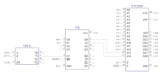
Here the right hand half of the 139 is not used, and instead the two bit address forms the upper address lines of a 32K ROM chip. This gives the same result as the four ROM chips in the previous design, but at a cost and complexity saving.
Of course, the next logical step is to connect up an extra data line to the latch, and use a 64K ROM chip, and as if by magic, you have a 64K ROM bank cartridge, selectable by writing a 3 bit address to the IO port.
But why stop there? change that latch to a 74LS273 8 bit latch and the EPROM to a 27C080 1MB ROM and you have a 1MB banked ROM cartridge selectable by a 7 bit address written to the IO port.
Why not 8 bit? Well, at some point someone decided to use the eighth bit as an enable. This is used to drive the /EXROM line on the cartridge port which enables the 8K space we have been using. This is useful for a program which loads from ROM into RAM and can then disable the ROM elements and run entirely from RAM. This is often used with a compression step to fit even more into the ROM chip. The decoding can also be changed to stop further writes to the latches, but I have not shown that for clarity.
At this stage, when you are implementing a practical cartridge, there are other things to consider, which add complexity to the simple schematic above. Mainly it is adding jumpers to allow different ROM chips. Borrowing the table from the previous blog post, on the Marina 64 cartridge we removed a few of the less common chips to give a 32K -1MB range with only a single jumper to select 28 pin or 32 pin ROM chips.
So there you have it, that sort of bank switching is common on larger ROM cartridge (such as those produced in the 1980s by Ocean), and on modern multicarts (such as the VIC20 Penultimate Cartridge).
A production surface mount version of the Marina 64 32K-1MB banked ROM cartridge is available from TFW8b.com.

Sunday 9 February 2020

Marina64 1MB Banked ROM Cartridge for C64


This is the Marina 64, a new 1MB banked ROM cartridge for the Commodore 64 (and Commodore 128 and SX-64).
This is based on the Magic Desk cartridge. This was a Commodore product back in the 1980s which was an early attempt at a desktop operating system. With a literal desktop (possibly the origin of that?).
There was a file manager, calculator, and a very strange word processor that was like a virtual typewrite simulator where as you typed, the page of text moved to the left, creating a document 80 characters wide on a 40 column screen.
This didn't catch on, and was superseded by GEOS and things like that. However, it lives on in the hardware that was used. I haven't been able to find any pictures of the original Magic Desk 1 cartridge, but it consisted of four 8K ROMs, and two TTL chips. These formed a simple bank switching mechanism to allow the four ROMs to be accessed through a single 8K window. On boot, the first ROM would be selected, and the C64 would boot as if it were a normal 8K cartridge. When the program needed to access one of the other blocks of code, it would write to an IO address which would select a different ROM from the four available.
At some time in the past, a thought must have occurred to someone that it would be a good starting point for their own cartridge. The C64 was limited to 16K ROM in a cartridge, so this was a way to get a 32K game in cartridge form. Another thought would have occurred that this could be achieved with similar logic and a single ROM chip, selecting one block or bank of 8K from a single 32K ROM chip (not sure if Commodore ever did this or it was later clones). Further thoughts could have been along the lines that the bank is selected by writing a byte to the IO port, and only the first two bits were used to select the bank, so a larger ROM chip could be used by latching more bits of the byte written to the IO port to use to select the bank. (There will be a more detailed look at this in a later blog post). There are now many variations of the design of 'Magic Desk compatible' cartridges, and when looking for a cartridge for larger games for The Future Was 8 bit '999' range of cartridges, this seemed a well established and well supported way to go.
My first attempt was a 'developers edition' cartridge, really just an in house testing tool. This had the ROM socket, and two TTL chips. One of these is simple decoding logic, the other latches the number of the bank selected. Here I am using a 74HCT273, so it latches the whole byte written to the port. The original design used a 74LS174 which can only latch 6 bits. Most of the versions of the design I have seen online had lots of jumpers. TFW8b doesn't like jumpers (he asked me to add here he also hates cardigans), so I looked into which ones we actually needed.
This is the result of my analysis of the various options for common EPROM types. The first jumper I got rid of was the one on the /EXROM pin. This was there to disable the cartridge so it could be programmed in system. I didn't see this as a requirement of this implementation of Magic Desk, at 300 bytes per second out of an IEC drive, it would take just under an hour to program a 1MB ROM chip, so I would recommend just using a standard EPROM programmer where it takes a couple of minutes.
The remainder of the jumpers were selecting a bank address or 5V for the upper address lines on smaller chips. The 27C64 and 27C128 aren't really relevant here as they can use plain cartridge PCBs for 8K and 16K titles. By discounting those, and the writable chips version the 28C64, and the 28C256 with it's address lines in a different place, and the largest writable 39F series chips, you get down to a single jumper, one to select if the ROM is 28 pin or 32 pin.

EPROM
Jumper
Banks
Capacity
27C256
28 pin
4
32K
27C512
28 pin
8
64K
27C010
32 pin
16
128K
27C020
32 pin
32
256K
27C040
32 pin
64
512K
27C080
32 pin
128
1M

This is a common differentiator with TFW8b products. This will work for most people, most of the time. For the few who want to use different chips, or write in system etc. other products are available, but we try not to over complicate the main product for the average user. I was asked about the need to stack two 512K chips to get 1MB. I have seen a cartridge which requires this, but I don't see why that is necessary when you can use a single 27C080 1MB chip.
This is the prototype of the cartridge, dubbed the Marina 64 (for obvious reasons). These boards are available now as a bare PCB from TFW8b.com. A production version will be available soon, with surface mount ICs pre-assembled, and an activity LED, which shows when the cartridge is active.
Naturally, the cartridge PCB is designed to fit into the TFW8b.com C64 Stumpy Cartridge Cases. Available in a range of tasteful colours (and pink), and also available blank labels for your own titles.
One of the benefits of going down the Magic Desk route, is there are a number of programs around to generate compilation cartridges and self extracting programs to work with a Magic Desk cartridge, and these can be previewed and tested in the Vice C64 emulator.
A good example of this is the Magic Desk Cartridge Generator v3.0 by Žarko Živanov. This is a python script which can be used to compile a cartridge from normal PRG files. The script generates a menu program which allows you to select a program, which is then decompressed into RAM. The programs can span multiple banks, and with 1MB capacitor you can fit dozens of programs on a single cartridge.
Another option is if you have a single large prg file, you can use a program such as the C64 Cartridge Creator tool 1.0.0 by Solo761. There is no menu in this case, it just copies the prg file from the ROM cartridge into RAM and starts it running. None of these options are suitable for programs which require multiple files (for example disk games), only single prg files.
Update - The production versions are available now Marina64 PCBs from TFW8b.com.

Update - see the following blog post for more details on How banked ROM cartridges work.