Sunday 31 July 2022

Commodore plus/4 7 pin power conversion

The Commodore plus/4 uses an unusual 4 pin square DIN plug for it's power. 

Into this you would normally plug a Commodore plus/4 power supply. However, these are known to not be very reliable.

One solution to this is to cut the lead off a plus/4 power supply and wire it to your own supply. There is an alternative if you have one of the earlier revision boards.

The original design plan for the plus/4 was to use the same 7 pin DIN power socket as the Commodore 64 and later VIC20s. The designer Bil Herd apparently kept changing the schematic to a 7 pin and production kept changing it back to the 4 pin.

It seems this may have continued until after the PCBs were designed, as the earlier boards (assembly no 310463) have some extra pads under the 4 pin socket. Later PCB revisions (e.g. assembly no. 250455) sadly do not have these extra pads.

If you desolder the 4 pin DIN plug, you get a pattern oh holes which might look familiar if you have worked on a Commodore 64.


If you look at the 4 pin DIN and compare it to a 7 pin DIN, you will see various pins in common.


And if you offer up a 7 pin DIN socket to the plus/4 PCB, you will see it fits perfectly.

You might be concerned that the pads would not be wired to the correct signals, but no, all the pins are already wired up correctly.


Pins 1, 2 and 3 are ground. Pins 4 and 5 are 5V DC. Pins 6 and 7 are the two 9V AC connections.

The poor 4 pin DIN socket looks sad now that it has been consigned to the spares bin.


They always remind me of the Cubes from Terrahawks.

When reassembled, it fits right in. 

One objection to this arrangement could be that it is possible to mix this up with the 8 pin DIN video connector.


However, they sold the Commodore 64 with that combination for years, and I don't think I have heard of anyone trying to power a C64 from "the other power socket" on the back.

Now that you have a 7 pin power connector on your plus/4 what should you plug in? 

Well, absolutely not a Commodore 64 power supply!

I use this aftermarket one from the 80s. It has severed me well over the years and is still solidly reliable.


I am not sure what brand it is, it just says it is suitable for computers requiring those voltages.


Inside it is pretty much as simple as it could be, mainly a large transformer.


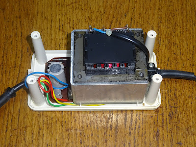
The circuit is 4 diode bridge rectifier, a couple of smoothing capacitors and a 7805, the only embellishment being a hard wired fuse.


The date code looks like 1987.

Interesting to note the plug actually has only 4 pins present, as was common on the Commodore versions as well.

Shout out to the very 80s mains plug this one has always had.


7 pin conversion - check. 7 pin power supply - check. Time to test it out.

And there you go, one plus/4 running from a more reliable power supply.

I left the plus/4 running Diag264, and it seems happy, all the voltages look good, so that's job done.


I don't normally use a plus/4, the keyboards always seem to need attention. This one about half the keys need to be pressed very hard several times before they wake up. 

For any TED testing, I normally use a Commodore 16 with a 64K upgrade - see the post where I did that.

http://blog.tynemouthsoftware.co.uk/2019/02/commodore-16-64k-upgrades.html

However, it's always handy to have one around so I can use the built in software.

OK, maybe not.

Update

I noticed the label on the power supply was looking a bit tatty, so I made a new one.


I started with a patched up photo of the original, then made that black and white to more clearly see the letters and then replicated them as best as I could. It was difficult to find a font where the S was closer to an 8 and the y had a straight stroke. In the end, I couldn't get an exact match, but Calibri came close and the y was more noticeable that the S.

I did make one slight change, I couldn't leave it as 1.5a, I had to change it to 1.5A. I had to adjust the  kerning on the VA with an extra 25% between them to get that to line up, everywhere else was standard.


There, that's much better.


Advertisements

If you want to see more posts like this and behind the scenes progress on new projects, you can follow along and support me on Patreon:

https://www.patreon.com/tynemouthsoftware

Saturday 23 July 2022

New VIC20 Cartridge PCBs

A new VIC20 Cartridge PCB is now available from TFW8b.com


The new design came out of two separate points in a conversation that took place before ordering more of the existing boards.


We currently have one PCB which can be either an 8K or a 16K ROM cartridge for the VIC20, and a second PCB which can only be a 32K ROM cartridge.


The request from TFW8b was "could you do a combined 8K+16K+32K board"? I guess so, but there are already too many jumpers on the 8K/16K board, and to switch to 32K mode would need an extra couple of jumpers at least.

The second point raised is these are half size board, only big enough to pass the screw hole and the two supports.


This is not unusual as most of the Commodore game cartridges were that size.


Comment was also made that these were sometimes a little loose, and not as well anchored as the Penultimate Cartridge PCBs, which fill the whole case.


The second point was "Could I make these cartridges full size as well?"

Well I could, but there would be a whole load of space left. 

I did consider putting a whole load of jumpers up there to do a combined board, but then I had a silly idea.

Why not put both cartridges on the same board?

That should fit within the outline of the Penultimate cartridge, with some space at the side.

There seemed to be enough space for both boards, wired in parallel to the edge connector, so I had a go.


You wouldn't fit the chip for both types on the same board, just one set.

For an 8K or 16K cartridge, you would use to the top half of the board and ignore the 32K section.


For a 32K cartridge, you would use to the bottom half of the board and ignore the 8K / 16K section.


That was a full size board (as requested) and could do 8K, 16K or 32K (as requested), but rather than having to set lots of jumpers to switch between the cartridge types, you just fit the chips in different places.

I routed all the traces, and then moved a few things around a bit. I remember there was a central reinforcing bar in the lid of the case, but I had forgotten there was a similar thing along the top, exactly where I had placed the top ROM chip.

Plan B was to rotate the ROM chips 90 degrees and place them at the sides of the board.


I was also rather pleased with the way the traces were laid out. 


And there you have it, the new cartridge PCB. 

ROM chips and ROM blocks

The VIC20's address space is split into 8 8K blocks. Blocks 1,2,3 and 5 are reserved for the cartridge slot, and these cartridge PCBs can place ROMs in any of these blocks. When looking at ROM files, you may see things like 5 or blk5, or A0 or A000 in the filename to determine where the file goes. You sometimes find ROMs as .prg files which are 8K + 2 bytes (8194 bytes), and the extra two bytes are at the start and indicate the address (A000 for example). To use these, first remove those two extra bytes to reduce the file size to exactly 8K (8192 bytes).

Address range
Block
Use
0000-1FFF
0
5K RAM
2000-3FFF
1
8K ROM Block 1
4000-5FFF
2
8K ROM Block 2
6000-7FFF
3
8K ROM Block 3
8000-9FFF
4
Video and I/O
A000-BFFF
5
8K ROM Block 5
C000-DFFF
6
8K BASIC ROM
E000-FFFF
7
8K KERNAL ROM

ROM chips from 27C64 through to 27C512 can be used, as long as the ROM chip is at least as large as the ROM image. If the ROM chip is larger than the image (e.g. 8K ROM in 27C256 EPROM), then it should be placed at the top of the ROM chip (e.g. 0000-5FFF unused, 6000-7FFF 8K ROM image). Note 28C64B can be used, but 28C256 is not suitable as it's A14 pin is in the wrong place.

There is a list of addresses on the back of the PCB, so you can't lose it.

Construction

Construction should be fairly straightforward. There is space to use sockets if you wish, or you can solder the chips direct to the board if you are confident they are programmed correctly. If you fit a chip, you should fit the corresponding 100nF decoupling capacitor, either an axial ceramic through hole capacitor, or there are pads on the back of the PCB to fit a 1206 ceramic surface mount capacitor.

As it says on the board, fit parts only on the 8K/16K side OR the 32K side, do not fit both.

8K Cartridge


To make an 8K cartridge, use the left hand ROM socket and fit the 8K jumper in place of the left hand 74LS08 logic chip. The lower bank jumper is set to 8K mode (there is no lower bank), and the upper bank can be 2, 3 or 5. It is almost always 5, as if a cartridge ROM is detected in block 5, it will automatically start on power on. 

The 8K ROM image should be burned to the EPROM at the following addresses.

Address range
27C512
27C256
27C128
27C64
0000-0FFF
-
-
-
8K Block 2/3/5
1000-1FFF
-
-
-
2000-2FFF
-
-
8K Block 2/3/5
3000-3FFF
-
-
4000-4FFF
-
-
5000-5FFF
-
-
6000-6FFF
-
8K Block 2/3/5
7000-7FFF
-
8000-8FFF
-
9000-9FFF
-
A000-AFFF
-
B000-BFFF
-
C000-CFFF
-
D000-DFFF
-
E000-EFFF
8K Block 2/3/5
F000-FFFF

4K Cartridge

It is also possible to build a 4K cartridge, using the 8K settings above. The 4K ROM image should be at the start of the 8K bank, and the 8K bank should be at the top of the ROM as above.

Address range
27C512
27C256
27C128
27C64
0000-0FFF
-
-
-
4K Block 2/3/5
1000-1FFF
-
-
-
-
2000-2FFF
-
-
4K Block 2/3/5
3000-3FFF
-
-
-
4000-4FFF
-
-
5000-5FFF
-
-
6000-6FFF
-
4K Block 2/3/5
7000-7FFF
-
-
8000-8FFF
-
9000-9FFF
-
A000-AFFF
-
B000-BFFF
-
C000-CFFF
-
D000-DFFF
-
E000-EFFF
4K Block 2/3/5
F000-FFFF
-


16K Cartridge


To make a 16K cartridge, use the left hand ROM chip and the left hand 74LS08 logic chip. The 16K is split into two 8K blocks. The lower bank can be block 1, 2 or 3. The upper bank can be block 2, 3 or 5. Select the upper and lower bank with the jumpers. Most use 1+5 or 3+5 (except Scott Adams text adventures which use 1+2)

The 16K ROM image should be at the top of the ROM chip

Address range
27C512
27C256
27C128
0000-0FFF
-
-
8K Block 1/2/3
1000-1FFF
-
-
2000-2FFF
-
-
8K Block 2/3/5
3000-3FFF
-
-
4000-4FFF
-
8K Block 1/2/3
5000-5FFF
-
6000-6FFF
-
8K Block 2/3/5
7000-7FFF
-
8000-8FFF
-
9000-9FFF
-
A000-AFFF
-
B000-BFFF
-
C000-CFFF
8K Block 1/2/3
D000-DFFF
E000-EFFF
8K Block 2/3/5
F000-FFFF


32K Cartridge

To make a 32K ROM cartridge, use the right hand 74LS08 and right hand ROM chip. There are no jumpers to set, the ROM is always mapped as blocks 1+2+3+5.

The 32K ROM image should be at the top of the ROM chip. 

Address range
27C512
27C256
0000-0FFF
-
8K Block 1
1000-1FFF
-
2000-2FFF
-
8K Block 2
3000-3FFF
-
4000-4FFF
-
8K Block 3
5000-5FFF
-
6000-6FFF
-
8K Block 5
7000-7FFF
-
8000-8FFF
8K Block 1
9000-9FFF
A000-AFFF
8K Block 2
B000-BFFF
C000-CFFF
8K Block 3
D000-DFFF
E000-EFFF
8K Block 5
F000-FFFF


Cases


These fit snugly in the TFW8b VIC20 cartridge cases. There are two places where a reset button could be installed if you need one and have a hole in the case.


I think they have turned out rather nicely.


Advertisements

The new cartridge PCBs and cartridge cases are available from The Future Was 8 bit:

Patreon

You can support me via Patreon, and get access to advance previews of projects and behind the scenes updates. This now also includes access to my new Patreon only Discord server for even more regular updates.

https://www.patreon.com/tynemouthsoftware