The products and services mentioned within are no longer available.
This post has been left for historic information. The PET microSD is no longer in production. The replacement SD2PET is available now, more information on the pre-order page.
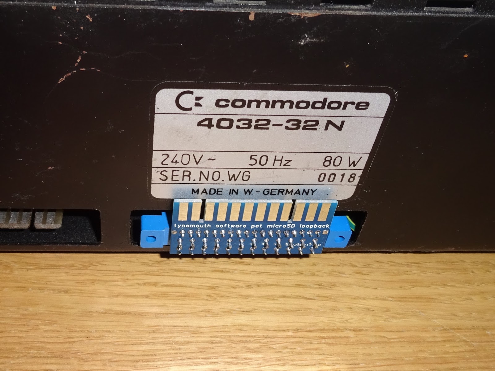
I've been updating the design of the PET microSD, and there are now three different versions to chose from, depending on how you want to connect it, and to what machine. All of these plug into the rear edge connector of a PET from a 2001 up to an 8032 (or variations of the 8032 such as the SuperPET 9000). See later for information on 2001-8 and 8032-SK support.
OPTION 1 - PET microSD v1.2 horizontal. The two boards at the top make up the original style board, currently on V1.2. This plugs directly into the IEEE-488 port on the rear of the PET. These are still available, and still the best choice for many users.
The board needs 5V power and that is supplied from the datasette port, with a passthrough connector to attach a datasette. This means it can be moved from PET to PET and does not need the case to be opened. Just plug the boards into the back.
The V2.0 boards provide some alternative mounting arrangements, and a few changes. Firstly, since these boards aren't sticking out the back, they don't need to be as small, so I've gone back to a slightly larger boards with all the parts on the top side, so the backs of the boards now only contain the serial number and firmware version info.
Secondly, rather than tap the 5V power rail, I've added a DC-DC converter on to the board, so it can be powered from any supply from 7v to 22v. There is a handy connector, J11 on the PET board, near the back of the case. This is designed to supply unregulated 9V to add on boards, such as the 64K RAM board.
The V2.0 PET microSD boards have a short cable with a 7 pin connector. 9V is on the centre pin, so it can fit either way around to avoid any problems. If you have a board which already uses this connector, I can supply a longer lead with a clip on the end to attach to one of the reservoir capacitors.
OPTION 2 - PET microSD V2.0 vertical. The first of these new boards is a vertical version, think ZX81 RAM pack, only slightly larger capacity and no RAM pack wobble.
This plugs into the back of the PET and the power cable plugs onto J11 inside the PET (2001N onwards). It takes up very little space and allows easy access to the microSD card. This is a good choice if your PET is close to the back of the bench.
OPTION 3 - PET microSD V2.0 internal. The second new board is much requested, one that can be installed inside the PET. OK. It's not entirely internal, there is no internal IEEE-488 header on most PETs, so it has a small loopback board that plugs into the back. I'll probably remove the pass through connector in the next version of this to make it half that size.
Inside the PET, the 18 way socket on the loopback board is just visible above the connector. There is just enough space for this to fit through easily,
The PET microSD fits onto this header and also the J11 power connector as before.
This is a good option if you want it hidden out of the way and don't need to remove the microSD card very often, or are happy to open the PET to change it.
This shows the PET microSD V2.0 internal mounted onto a 4032 board outside of it's case to get an idea of how it all fits together.
The 8032-SK and 8096-SK do not have rear edge connectors, but they do have the same 8032 board, and the edge connector is internal. This board is can be used internally in an 8032-SK, with the rear panel cable now plugging into the top of the loopback board.
PET 2001
All the versions of the PET microSD can be used with the original 2001, but 2001's with BASIC 1 need to be upgraded to BASIC 2 or BASIC 4, you can use one of my ROM/RAM boards to have a configurable BASIC 1/2/4 ROM and 8/16 or 32K RAM upgrade.
The original 2001 does not have the 7 pin connector, so I would have supplied a longer lead with a clip on the end, this attaches to the 9V rail, and the easiest place is on the leg of the reverse protection diode, the furthest leg from the corner of the board.
Which one do you choose? Well choose 1 if you want to move it around between PETs or easily remove it, or don't want to open the PET case. Choose 2 or 3 if you are short of space, or prefer less wires around the back. Choose 2 if you need access to the SD card, Choose 3 if you don't plan to change the card often, or are happy to open the PET as required. Not all PETs support all options, so see the table of which PETs support which boards, which also has buy it now links.
2022 Update: I have since designed a much nicer SD drive for a PET. The SD2PET is available from The Future Was 8 bit
The products and services mentioned within are no longer available.
This is a board which plugs into the 6502 CPU socket on something like a Commodore PET and can selectively replace the onboard ROM or RAM. I've been making these for a while, and as with all of the boards I make, I keep refining the designs. Adding new features I find I need, or taking requests or suggestions.
These are the new, red V3.1 boards, and feature an activity LED, reset switch. There are three scenarios where one of these boards is useful, as a diagnostic tool, as a ROM/RAM replacement or as a system upgrade. The original use is as a diagnostic tool. ROM and RAM are common causes of failure on vintage computers, and this is an easy way to rule out problems with the original ROM or RAM, buffering, multiplexing or address decoding. If it turns out there are faults with the original ROM or RAM, and replacements are not available, or too expensive, the board can be left in place. In these situations, you can remove all the onboard ROM and RAM and just run with the ROM/RAM board, reducing power consumption and heat generation inside the case.
The third use comes with older PETs with BASIC 1 or 2, or with less than 32K of RAM. The ROM/RAM board can contain multiple ROM images, so it can be used to upgrade these systems to BASIC 4 and 32K or RAM, or any combination down to BASIC 1 and 8K. This is how my 2001 system is setup.
One feature I tried to add to the previous version, but couldn't get working, was selective ROM replacement. This worked fine on the VIC 20 version, but not the PET one. With help from Dave Mercado, I've found the issue I was having appears to be with the compiler I was using, so I've rewritten the GAL equations for the board to get around the problems, and it is now possible to selectively replace the onboard ROMs.
The idea is you have a system which is not booting, set the board to replace all the ROM and RAM and see if it boots. If not, then you it's back to checking power, clock, reset etc. A lot of the time, that will be enough to get the PET to boot. You can then turn off the RAM and see if it will run with it's own RAM. If not, you need to sort out RAM problems. There are two banks of 16K, and these can be selective controlled, so you can enable the lower bank to get the system to boot and then test the upper bank (see a previous repair on a 4032 for some techniques you can use).
Once the RAM is sorted, you can look at the ROM. You can select multiple ROM images (up to 16), but with previous versions of the board, it was either all ROMs replaced or none. So if a ROM fault was detected, you needed to identify the culprit by other methods. Now you can enable only one ROM on the board at a time, with the rest replaced, to see which ones work and which ones will not boot. The board can also be used on things such as the VIC20, anything with a 6502 CPU, apart from systems with banked RAM or multiplexed video RAM.
The new DIP switch settings are as follows:
RAM mode
RAM mode
ROM mode
ROM mode
ROM mode
ROM selection
ROM selection
ROM selection
ROM selection
On the 2001 version, the RAM mode switches select 0K, 8K, 16K or 32K of RAM.
Switch 1
Switch 2
RAM mode
0
0
No RAM is replaced
1
0
8K RAM
0
1
16K RAM
1
1
32K RAM
On the normal PET version, the RAM mode select bank 0 enable or bank 1 enable or both.
Switch 1
Switch 2
RAM mode
0
0
No RAM is replaced
1
0
lower 16K replaced
0
1
upper 16K replaced
1
1
both banks replaced
The rest are the same for both versions. The ROM mode switches select which ROMs are replaced. For example, with switch 5 only on, the KERNAL ROM is being tested. All ROMs are replaced by the ROM/RAM board, apart from the range 0xF000-0xFFFF, which is the UD6 socket on a 4032/8032 and the H4 and H7 sockets in the 2001. The 2001 uses pairs of 2K ROMs in identically wired sockets, one with an active high enable pin, one active low. Later PETs use a more conventional arrangement of a single 4K ROM per block
Switch 3
Switch 4
Switch 5
ROMs replaced
Range
2001
8032
0
0
0
None
-
-
-
1
0
0
All
-
-
-
0
1
0
All but Editor
E000 - E7FF
H3
UD7
1
1
0
All but Options
9000 - AFFF
-
UD11 / UD12
0
0
1
All but Kernal
F000 - FFFF
H4 / H7
UD6
1
0
1
All but BASIC B
B000 - BFFF
-
UD10
0
1
1
All but BASIC C
C000 - CFFF
H1 / H5
UD9
1
1
1
All but BASIC D
D000 - DFFF
H2 / H6
UD8
The ROM selection sets the higher address bits on the ROM. If a 27256 is fitted, a single 32K ROM image is available. With a 27C512, two images are selected via switch 6. With either of these, a jumper should be fitted next to the ROM socket to enable power to pin 28. This is not required for 32 pin ROMs. With a 27C010, 4 images are selected using switch 6 and 7. With a 27C020, switches 6, 7 and 8 select the 8 images, and if you can find 16 ROM images, then it's a 27C040 and switches 6-9.
Currently, I supply a 4 ROM set with 2001 boards:
Switch 6
Switch 7
ROM Selection
0
0
PET tester
1
0
BASIC 1 No CRTC Normal keyboard
0
1
BASIC 2 No CRTC Normal keyboard
1
1
BASIC 4 No CRTC Normal keyboard
The normal PET version gets those same 4 non-CRTC based ROMs, as well as 4 CRTC versions, 40 and 80 columns with business or graphics keyboards
Switch 6
Switch 7
Switch 8
ROM Selection
0
0
0
PET tester (No CRTC)
1
0
0
BASIC 1 No CRTC Normal keyboard
0
1
0
BASIC 2 No CRTC Normal keyboard
1
1
0
BASIC 4 No CRTC Normal keyboard
0
0
1
BASIC 4 40 Column CRTC Normal keyboard
1
0
1
BASIC 4 40 Column CRTC Business keyboard
0
1
1
BASIC 4 80 Column CRTC Normal keyboard
1
1
1
BASIC 4 80 Column CRTC Business keyboard
Various sockets have been used on the PET over the years, and it is difficult to find a way to fit with all the different types of socket, I've ended up with two options.
For most cases, I use the type on the left. These turned pins will fit into most sockets. Some of the single wipe sockets (particularly the white ones) aren't that good, particularly after the CPU has been inserted and removed a couple of times. With those you can push a turned pin socket into the existing socket, to get a good contact, but you may have to bend the contacts back or change the motherboard socket if you want to remove the turned pin socket at a later date.
You can fit the pins to the bottom of the ROM/RAM board two ways around, to give two different pin lengths, or stack 40 pin turned sockets to give extra height over other socketed chips.
On the early 2001 models, the socket have high shoulders so these pins will not fit. For those, I have a version with long thin pins that slide into those sockets.
Update:
The pins fitted to the current stock of boards suit all socket types, so the long pins are no longer required.
These boards are available to buy from my Tindie Store, alongside the new smaller PET ROM RAM board.
2022 Update: The redesigned small version of the PET ROM/RAM boards are still available from TFW8b.com
The products and services mentioned within are no longer available.
Commodore PET's never fail to find new and interesting ways to fail. This is a new one on me. It started as a normal repair, black screen, no beep, usual 8032 faults, but took a lot longer than usual.
So far, so good, looks OK in general. One 4116 has been removed, and some tracks damaged and repaired on the back. I checked those out, no problems with that, all continuity fine.
My usual first tests are power, clock, reset, all the necessary things to get started. Power was OK, all the voltage rails reading in tolerance. Clock and reset however, were a little odd.
The two traces shown are the reset line and the clock out from the CPU. The top one is the reset line, and it's really not meant to do that, but I'll come back to that. The first thing to deal with is the clock. It looks fine, a nice clean 2MHz clock. The thing is, the PET is meant to run at 1MHz.
The frequency counter confirms this, 2MHz. Everything else tells me it should be 1MHz. I tracked this down to a 74LS393 used as the clock divider. This was meant to take the 16MHz clock (which was measured at 16MHz) and divide it down to 8MHz, 4MHz, 2MHz and 1MHz for the system clock. It had other ideas, and it's outputs were 16Mhz, 8MHz, 4MHz, 2MHz. I presume the first stage had failed and passed the full 16MHz down to the second. Replacing that returned the system to it's non overclocked state. I don't know how long it had run overclocked to 2MHz, but many of the parts would not have been designed for that.
The reset was still pulsing though. On the PET it's a 555 timer set to generate a short reset pulse, this is buffered by a 74LS04, and then a 7417 open collector buffer is used to supply the reset line to the CPU, the I/O chips and the video CRTC. Tracing the signal through, the 555 was fine, and the signal out of the 74LS04 was OK, but the output of the 7417 was being pulsed low. It's open collector output, so it cannot drive high, it relies on a pull up resistor. This allows you to add other OC outputs or switches to the same line to reset the system.
I checked the resistor (R15) that pulls it high, and it measured fine, and putting another resistor in parallel changed the signal a bit, but not much. I replaced it anyway, along with the 7417. This made no difference. With the 7417 removed, I could see the line was being pulled down elsewhere. Another gate on the same chip is used to generate the IFC signal on the IEEE-488 bus, which was also fine. The only other things on there are the five 40 pin chips. With the CPU removed, something is still pulling the line down, so I started with the usual candidate, the 6545. That didn't change it, next the keyboard 6520. That seemed to fix the reset problem. With those replaced, the PET wasn't booting, so I installed a ROM/RAM board to bypass the onboard ROM and RAM. Still nothing. Checking the IRQ line, that was also doing odd things. I removed the 6522 and the other 6520 and that seemed to fix that. Once those were all replaced, it booted with a chirp and something on the display.
When you get banding like that in blocks of 8 or 16 etc. It is often down the the address multiplexers. Checking the outputs of these there were a few stuck and some doing strange things. I removed and tested the three 74LS157's and all were faulty. Replacing those changed the display, so progress was being made. Replacing the 74LS166 got rid of the flickering around the edges and finally a display.
The screen was full of @ symbols (0x00 in PETSCII), but there was some writing on the screen, and you can just make out 'commodore' in there. Some of the bits were wrong. I checked around various parts of the board, and it seemed that some of the data lines were always low. The ROM/RAM board has an isolated databus for it's ROM and RAM, so that wasn't affected. So it was something on board, one of the buffers, the RAM or the ROM. The only socketed ROM chip was UD7, the editor ROM, and that was a bit warm, so I removed that and it fixed some of the faults, and checking with the PET tester ROM, it initially looked OK.
But if you check carefully, you can see it's not right. It's repeating chunks of the character set. Where are the numbers? Checking the PETSCII codes of what was displayed and what should have been, it appeared that bit 5 was stuck low. I desoldered the other 4 ROMs and tried again.
Excellent, so all the video side was now working. The ROM/RAM board was still required, as the ROMs had been removed and the onboard RAM didn't appear to be working. With the ROM/RAM board, I can separately enable the upper and lower bank of memory, so I replaced the lower bank, which allowed it to boot, but left the on board upper bank enabled. Using the POKE and PEEK methods I described in a previous repair, I was getting results that showed that 5 of the 8 bits were faulty. I was hoping it would be better than that. It could be addressing issues causing that, or it could indeed mean that 5 RAM chips were faulty. To test this, I removed one chip and tested it on my Spectrum DRAM tester.
Yes, that's faulty. Putting a working DRAM chip into the PET confirmed this as it now looked like 4 of 8 bits were faulty. I replaced the other 4 and found the same, the chips were faulty, and the replacements reduced the error count. I then had the whole upper 16K bank working.
The lower was also faulty, so I swapped the bank select resistors so I could work on the lower bank, but mapped to the upper 16K, leaving the lower 16K working so I could get into BASIC. Again, I was hoping for better, but the results showed 7 of the 8 bits were faulty. Given that, I removed and tested all the remaining RAM and in the end, 3 of the original chips were working, and the one that was replaced originally.
With a complete set of replacement RAM, I could disable the RAM on the ROM/RAM board and I let it run through various diagnostics. I had to load these from tape as the IEEE-488 port wasn't working, as can be seen in the 8296 diagnostic, the video RAM fault is because the 8296 has 4K of video RAM, and the editor ROM is different, but it's still a useful stability test.
With the RAM working, I tried replacing the ROMs and most of them seems to cause the bit 5 issue. I also tried a working set of ROMs, and although they didn't corrupt the screen, it wouldn't boot.
Checking the enable pins, they were all wrong, and tracing back through that found various faults in the address decoding circuitry. The 74154 was stuck with one output low, even with the NOP generator feeding in all possible addresses. That fixed most of the chips, but the enable for UD7 is gated to mask out the I/O area. Various issues where found with the decoding chips, some of the signals seem to stick at 1V for a while, rather than being clearly high or low. Replacing several other logic gates around that seemed to fix that, and I was able to run it without the ROM/RAM board for the first time.
The burn in tests ram for several hours without a problem. So what's left? the IEEE-488 is still not working. I checked the MC3446N buffer chips and guess what, all were faulty. Does nothing work on this board? With those replaced and it was loading files fine from a PET microSD board.
The final tally then, with the surprising exception of the video RAM and character ROM, pretty much everything else on the board was faulty. I retested the parts and most would not let the system boot as they were pulling down reset, IRQ or data lines, or doing odd things with the addressing. Something really bad happened to this board in the past. I don't know if it was static or a power spike or aliens. It may just have been bad luck that the clock divider failed and overclocked several parts to death, and the address decoding faults caused lots of chips to try to write at the same time and burn each other out.
Given the cost of a full set of replacement ROM and RAM chips, I'll be returning this board with empty ROM and RAM sockets and a ROM/RAM board installed. This keeps the cost down and the owner still has the option to fit a set or 4116s and EPROMs in future.
Update:
The board is now back with it's owner. Here is his video showing the board being reinstalled in the case.
Also see their videos covering restoring the case and keyboard.
The products and services mentioned within are no longer available.
Here's a quick preview of a couple of upcoming Commodore 64 projects.
Commodore 64 pseudo stereo dual SID
This was inspired by a video from GadgetUK, where he modified a dual SID board to run two SIDs in parallel. Normally the dual SID board is used to add a second SID and a different address, to generate actual stereo from suitable software. The idea with this mod was to place two at the same address, so they could be driven from normal software. You may think that there is no point in doing that, they will both sound the same? Well, there is quite a variation in the sound produced by different SIDs, and the idea here is to exaggerate that by using a 6581 from a C64, and a much later 8580 from a C64C.
I raised the issue of a possible problem with two parallel SIDs when it comes to reading, as both devices will be selected, and both would try to write back to the databus. I suggested adding an OR gate to the chip select of the second device, so it would only be selected when the chip was selected and it was in read mode (or since it's all negative logic, it would NOT be selected if either the chip was NOT selected OR it was NOT in read mode). I said this could be implemented with a simple diode OR, and in the followup video, that seemed to be working nicely once the pull down resistor value was sorted out. To avoid any issues with that, I've used a single gate OR gate here, rather than a diode OR.
There are a few differences between the 6581 and the 8580. The power supply, filter capacitors and audio output amplifier circuit are all different. So what I've done here is to ignore the C64's filter caps and fit these onboard. I also ignore the power supply and have onboard 9V and 12V regulators, with the power to be tapped from the main power supply filter capacitor. I've left the audio from the main SID going to the C64, but both audio signals are also buffered onboard and fed to the audio output jack.
Commodore 64 PLA replacement with EPROM
Replacing the commonly faulty Commodore 64 PLA with an EPROM is something I tried a few years ago, with mixed results. I also tried to make a replacement using two GAL chips, but didn't get very far with that.
Following another video from GadgetUK, he seemed to have more success using the EPROM method and adding a 68pF capacitor to the /CASRAM line. The issue here is that due to what could be considered a design flaw in the C64, the /CASRAM line needs to be delayed by about 25nS to allow the addresses to be ready in the multiplexer before they are loaded into RAM.
I've updated my board to have space to add a suitable capacitor. These probably needs to be tuned to each board, depending on the type of RAM used.
To make this more repeatable, I've added a quad OR gate to add a configurable delay. Each gate has a propagation delay of around 9nS, so with the jumper you can select to tap the signal after 1, 2, 3 or 4 gate delays. This will add 9nS, 18nS, 27nS or 36nS delay to the signal .These timings are approximate, but are typical values. I can also shorten or extend this by using a different logic family chip.