Saturday 30 August 2014

BT 741 Wallphone conversion

This is an old post, preserved for reference.
The products and services mentioned within are no longer available.

Time for a new phone. Apple or Android? Neither. One with a dial and a curly cord please. Back in 1979, we moved into a new house and it came with a brand new BT 746 phone. It's simple technology and still works well, and I've used it on and off for the last 35 years.
When originally supplied in 1979, it was wired directly into the house phone network, and sat in the hallway as the only phone in the house. The date code of 79/3 on the bottom confirms the date.
Sometime in the mid 1980's, the house was upgraded to a plug and socket system and the phone was retired to be replaced with one of those new fangled push button things. Sometime in the 1990's, I needed another phone, so converted this to work on the new system. About 5 years ago, I gave it a bit of a cleanup and a new curly cord. The parts were still available (I got mine from Abdy Antiques), and the new cord fitted perfectly.
It was an easy job with screw terminals at both ends. You can see the new handset cord on the left, and the original line cord on the right, just a bit dirtier.
The dial isn't the fastest way to make a call, it's ok for things like 1471 and local numbers, but I think mobile numbers would be a bit of a push. Now I find the need for another phone, out in the workshop, just on the edge of the range of the cordless DECT phones I use elsewhere. This time I went for the BT 741 model, the same sort of thing, but designed to be wall mounted.
I picked this one up on ebay, it appears to have been directly wired to some internal telephone system, but the great things about such simple elegant technology as this is it is just a case of changing the wiring inside to set it up for use on modern phone networks.
This is how it was wired, a bit more that usual going on there, but much of that is to do with the phone system it was wired to. The rest is pretty much standard and was so from the 1950's I think up until the mid 1980's. It's all well documented, the site www.britishtelephones.com  has lots of information, and here is the full circuit diagram.
Here is the 741 rewired for modern use, following the instructions on the site for 700 series phones. I made up a new line cord out of an old modem lead, but the rest was just screw terminal work.
Looking inside, I saw this dangling down, I don't think it's meant to be like that. But these things were designed to be serviced, so the dial mechanism folds down so you can see what is going on. Not quite the same as a glued shut iPhone.
This is the back of the Type 28 dial mechanism. Two things here, one the spring and screw were loose. Not sure if that was deliberate, or happened in transit. The other is the blue wire, which appears to be shorting out the switch. It may have been set like this to stop outgoing calls being made. Removing those and setting things back to how it should be, reassembled and tried again. Success, all seems well, and I always think the sound quality is better than the wireless phones. Give me wires any day.
I checked over my old phone at the same time, as you can see it's largely the same things, just the dial and hook are reversed. This particular 741 had an extra switch, although that is not connected. I can't think of anything for it to do, but I don't have a blanking plate, so I'll leave it there. It would have been used for an intercom or a door release or something. The 741 is a later model with a 4000 ohm coil. The 746 has the older 1000 ohm coil, so has a 3K3 resistor in series to reduce the loading for a modern phone. Still I like to use a microfilter on the line, so it generates its own ring signal.
All it then needed was a wipe over with a damp cloth and a new paper disk with the number on.
The 746 also got a new number disk and that was it done for another five years.
There is the question of approval for connection to BT, but the 741 dates from 1985 and was actually an 8741, so was designed to be used on the new network and has a green approved sticker. Has that been rescinded?

As with any of these posts, use your common sense, do not attempt things like this if you are not confident you know what you are doing. Although mains voltages are not present there are still over 30V and should be treated with care.

Thursday 28 August 2014

Commodore PET Repair Part 6 - 8032 to 4032 Fat 40 Conversion

This is an old post, preserved for reference.
The products and services mentioned within are no longer available.

This is the sixth part of the repair and restoration of a Commodore Pet 4032, you might want to start at Part 1. The story so far, the 8032 board is mainly fixed. I'm still using the ROM and ROM replacement plug in board for the RAM only. I'm still working on the RAM, even will a full set of known working RAM it's still failing, so I'm leaving that for the moment.
The original Pet I'm restoring was a 4032-32N, 40 column, 32K, 12" screen, Normal keyboard. Here it is about 10 years ago, yes that is a 3.5" floppy on the side, and there was a Pentium 75 inside. I don't have the original insides from that machine, so I have been repairing a board from an scrap 8032-SK, which is an 80 column board. This is one of the later 'universal dynamic pet' boards. Universal because it can be configured for 40 or 80 columns. Dynamic as it has 32K of Dynamic RAM. The earliest 2001 Pets had Static RAM. It would be much easier if this one had SRAM, as the DRAM is currently causing my problems.
Why would I want to convert the 80 column board down to 40 columns? Seems like a downgrade? Lots of reasons.
1) It was a 4032, so I would like it to be reborn as a 4032
2) It has the normal/graphics keyboard, and Commodore never released a machine as far as I know with 80 columns and this keyboard. Some software expects a certain keyboard and reads it directly rather than using the OS routines, so may get the wrong keys. So best to stick with 40N and 80B.
3) I already have a very nice, fully working 80 column pet, in the form of an 8032-SK (thanks, James - I'm still looking after it)
4) This may be the clincher, lots of the software is designed for 40 column screens, and doesn't look right in 80 column.
There are ways to reprogram the CRTC to switch to a pseudo 40 column mode, but it seems to be just the middle 40 characters of the 80 column screen. The characters are never going to get fatter whilst the dot clock of the 74166 is tied to 16MHz.
The conversion is relatively simple, change the link from 80 to 40.
Oh, but not just this one, there are 14 in total.
I've fitted sockets so I can change back to 80 column without recourse to a soldering iron. I may even look at switching via a number of 157s or even 4066s, with a dual ROM and a single change over switch. For the moment, I think I'll be happy with just the 40 column mode.
All but one of these is marked -40- or -80-, but J1 and J2 aren't. J1 is 40, J2 is 80. The Y/Z link at the bottom is 16K/32K mode, again not marked.
In 40 column mode, 5 chips can be removed, two buffers, a latch and 1K of the screen RAM. I've left the buffers and latch in place as they were still soldered in, but removed the SRAM as it was socketed.
The editor ROM needs to be changed, so I've blown a copy of the 40n50 editor ROM, time to switch on.
Looks like 40 columns to me. This is what space invaders looks like in 40 column mode.
It's now working as a 4032. Must get on with finishing this before I get carried away playing games. I may have said this before, but next it's time to finally fix the RAM.

Update: I have now removed the five chips (UB6-8, UC6-7) that wouldn't be fitted in a 4032 and made the mod permanent.


Sunday 24 August 2014

Commodore PET Repair Part 5 - Some ROMs a NOP Generator and a Logic Analyser

This is an old post, preserved for reference.
The products and services mentioned within are no longer available.

This is the fifth parts of the repair and restoration of a Commodore Pet 4032, you might want to start at Part 1. The story so far, the video circuits are now fixed, and the Pet is working, but only because it is using a ROM and ROM replacement plug in board. It's almost like the original design for the BBC, a main unit to provide I/O, video, keyboard etc., and a seperate unit with processor, ROM and RAM. Only in this case, they share a CPU. I could leave it like that. It is working, but I'd rather remove it and get back to the PET running on it's own.
I previously removed the ROMs as one was getting hot, and tested them. All but one were fine, as it happens the one that failed was the editor ROM. Quite useful as that is was 80 column, business keyboard, and when this is finished, I need to change that to 40 column, normal / graphic keyboard anyway. I've burned and tested a replacement for the moment. The old Dymo labels don't do well here, rather than 80 n 50, it looked more like 'BONSO'. Shades of Neil Innes?
The new label printer does a much better job, but the 40n50 will need to wait until I switch the video circuits to 40 column mode.
Putting the ROMs back and disabling the ROM side of the ROM / RAM board, but leaving RAM replacement enabled, it wouldn't boot, and one of the BASIC ROMs (UD8) was getting warm again. Checking with the 'scope, there appeared to be some conflict on the data lines. If I removed UD8, and powered on, it chirped, but there was nothing on the screen (since one of the BASIC ROMs was missing) and there were no conflicts on the data lines.
Nice verdigris on the J4 connector, but next to it, the ROM selection is controlled by a 74154 4-16 line decoder. This was one of the chips that had been damaged by corrosion and replaced, so that should be ok. I couldn't see anything out of the ordinary in normal operation, so time for another test device.
This is a NOP generator, it's a standard technqiue, and there are many ways to this, you can bend the pins of a 6502 and solder directly, or build a plug in ROM wired for NOP. I built this one using one of the spare ROM/RAM boards. The CPU is wired directly through to the socket on all but the data pins. On the ROM/RAM board, they are isolated by a tri-state buffer, here they are not connected through to the board at all.
Instead, they are hard wired to 0v and 5v in the pattern 11101010 (0xEA), which represents the 6502 NOP instruction. So whatever address the CPU tries to read, it will see 0xEA. When the CPU starts up, it will read 0xFFFC and 0xFFFD to get the reset vector. It will read 0xEA for both, so will set the program counter to 0xEAEA, and read the instruction there. That will read 0xEA, which is the 6502 op code for NOP, no instruction. So it will just increment the program counter and read the next instruction. That will also be NOP, and so it will continue until it gets to 0xFFFF where it will just loop around to 0x0000. And so on. What this achieves is the address bus continually cycles through the entire address range several times a second. So if you look at A0, you will see a 250KHz square wave, A1 will be 125KHz, down to A15 at 7.6Hz. Checking this showed that A3 and A4 both had an identical odd stepped pattern, and I traced that to a short on one of the ROM sockets. It still didn't work though, so the next step was to check the enable signals on the ROM chips.You can probe around the board with a 'scope or even a frequency counter, but I went for an eight channel logic analyser, so I could see the signals more clearly.
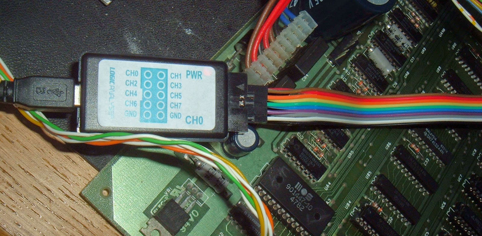
This is the cheapest of the cheap ebay job, which is a clone of the nice Saleae ones, and indeed copies their firmware, so their software thinks it is one of the theirs. It' a bit cheaply made and the probes were a bit rubbish, I tried to use them when testing the 74LS138 as part of the video circuit repair.
They stayed on long enough to get a couple of readings, but kept falling off. There were also problems with initialisation, I found the USB had to be plugged in before the target device was powered, otherwise the device would have power up due to parasitic power and fail to initialise. I suspect that may have fried the 7400 chip, as I was sure I had tested for that signal before, so I'm a little wary of it.
It did at least prove the display write signals were there, but I gave up in the end. I suspect the proper one will resolve these issues, and it has proved useful enough, so I'll probably buy one in time.
In order to test the enable lines, I've used breadboard jumper wires to make the connections, and that seems more stable.
This is the view showing the enable signals at the 7 ROM sockets UD12 down to UD6, and also A11, the highest address bit going to the ROMS. As you can see, the first ROM is enabled, then the second, then the third etc. There are two odd things. One, Channel 5 shows the signal to UD7, the editor ROM, and that has a glitch in it. However, that is meant to be there as that is the I/O region, located in the address space of that ROM, and the ROM is disabled when that area is accessed. The other thing is that channel 4 (UD8) is completely wrong. In fact, it's not channel 4, it's A10 by the look of it. I double checked my connections as A10 is pin 19, and the enable signal is pin 20. Checking further, I did find a short under the socket between pin 19 (A10) and pin 20 (enable).
With that fixed, the logic analyser showed the select lines were now how they should be. Time to reinstall the ROMs.
With the ROM/RAM board still in place to provide 32K RAM, but the ROM switched off so it uses the on board ROM, time to power on.
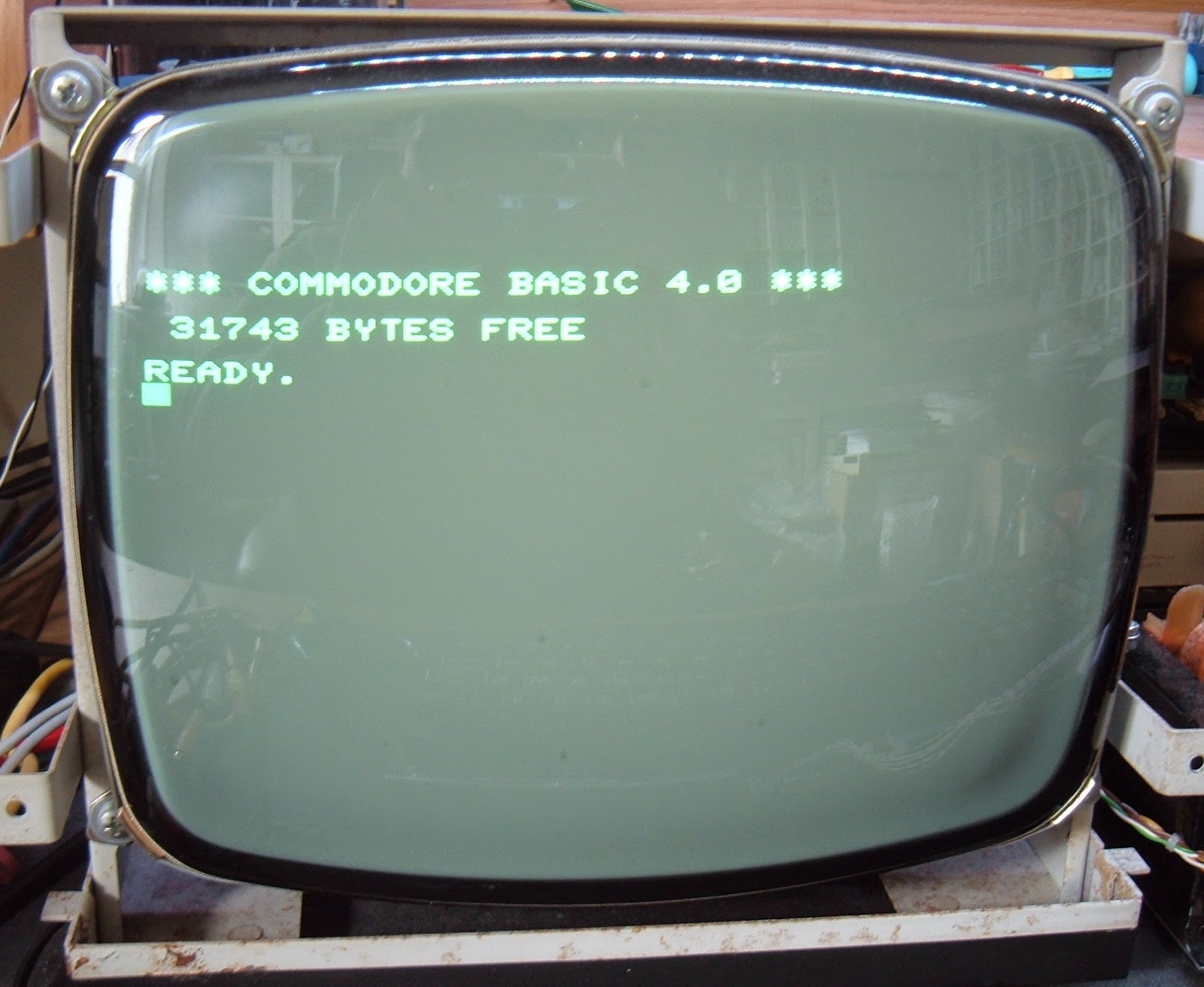
Success! The Pet is now using it's own ROMs, I/O and video circuitry. The next step is to fix the RAM....
(well, OK, the next step was actually the FAT40 conversion)

Friday 22 August 2014

ZX Spectrum Plus Replacement Keyboard

This is an old post, preserved for reference.
The products and services mentioned within are no longer available.

Ben Heck has recently been building a Spectrum portable computer (that's, a ZED X Spectrum by the way). In that, he used a matrix of tact switches for the keyboard. I remember trying something similar a while ago, for the Spectrum+. I took some photos, but didn't bother writing it up. I thought I may as well do that now.
Using the Spectrum + for USB keyboards is a bit annoying, as the extra keys can't really be used to full advantage, being wired as multiple keypresses on the original Spectrum 5x8 matrix, rather than extra keys. That means you get a right arrow key, but when you press it, it actually sends shift + 8 to the PC. Not really ideal. I do trap the shift keys and translate that to an arrow key, but it's still limiting.
The Spectrum+ has a an arrangement of separate key plungers, and beneath that, a rubber mat
Beneath that a membrane.
And finally, a backplate, sometimes plastic, sometimes metal with a paper insulating sheet.
For some reason the Spectrum plus membranes tend to be even more fragile that the original Spectrum ones, and have often failed. Whilst modern replacements are available, they have the same issue for USB keyboard use. A while ago, I looked at the option of getting a new membrane made with a different matrix, to allow the keys to be used separately for USB keyboards, but that worked out too expensive.
An alternative I tried was to make a PCB with tactile switches on, arranged in an arbitrary matrix to drive the USB keyboard controller. To test this, I made a prototype with veroboard. I placed the board behind a spare Spectrum + faceplate and marked the location of all the switches.
I installed the 58 tact switches as close as I could to the positions of the 58 holes.
These were wired as a 5x13 matrix and connected to one of my USB keyboard controllers.
The key caps and rubber mat were then installed as normal, with the board sitting below in place of the membrane and backplate.
The idea being that pressing the button presses the keyswitch. The end result? Well, I think it could be considered a partial success. It worked, was reasonably nice to type on, and had an expensive clicky sound. There was only one problem, a mechanical one.
The case wouldn't close. I plan to try a surface mount tactile switch version, with the USB controller built in. That should work, it's just going to be expensive to produce such a large PCB. Maybe one day I'll get around to it.
Update: I did design the PCB, but it wasn't practical. I have instead designed a replacement membrane.