Saturday 28 November 2015

Commodore 64 Pseudo Stereo Dual SID boards

This is an old post, preserved for reference.
The products and services mentioned within are no longer available.

One of the strong points of the Commodore 64 is it's sound chip, the SID (Sound Interface Device). There are all sorts of things use can do with these, and an interesting one I saw recently in this video from GadgetUK164, was the idea of using two SID chips, wired in parallel, to generate a sort of stereo signal. Both chips would be driven by the same digital control signals, but the outputs of SID chips do tend to be a little different, and so create a sort of stereo effect. This different is more marked if you use the version from the C64, the 6581 on one side, and one from the later C64C / C128, the 8580, on the other side.
I was concerned with wiring them directly in parallel, as the SID can be both written to and read, so when a read request is made, both chips will be trying to write to the data bus, which is not a good thing. We had a discussion in the comments on that video, and I suggested using an OR gate to generate the chip select signal for the second SID, most easily achieved in this case using a diode OR. In the followup video, he showed the modified board, with diode OR and pull down resistor.
The inverse logic is sometimes tricky, the chip select line on the SID is active low, so needs to be low to be enabled. The read/write line is low when writing, high when reading. Here we only need the second SID to be selected when there is a write request, so CS2 is low when CS is low AND R/W is low. Or to think of that the other way around, CS2 is high if either CS is high OR R/W is high, hence the OR gate. A variation on DeMorgan's law.
Or as a truth table:
CS
R/W
CS2
SID1
SID2
0
0
0
Write
Write
0
1
1
Read
-
1
0
1
-
-
1
1
1
-
-

I've designed some boards which include that additional logic. The digital side of the SID remains all connected in parallel, apart from the CS line on the second SID. I've used a single gate 74HCT32 here to OR the signal. There are four parts to the analogue side. Firstly, and least important here, are the two analogue inputs, these are used by the paddle controllers on the C64. These are wired to the first chip, and there values are read when using read commands. When read commands come in, the second chip is not selected, so ignores them. The second chips analogue inputs are tied to ground. There is a jumper to also supply the second chips CS line from another source, such as one of the decoded IO address select lines on the cartridge port, for software which supports dual SIDs. Even switch between the two options should you so desire.
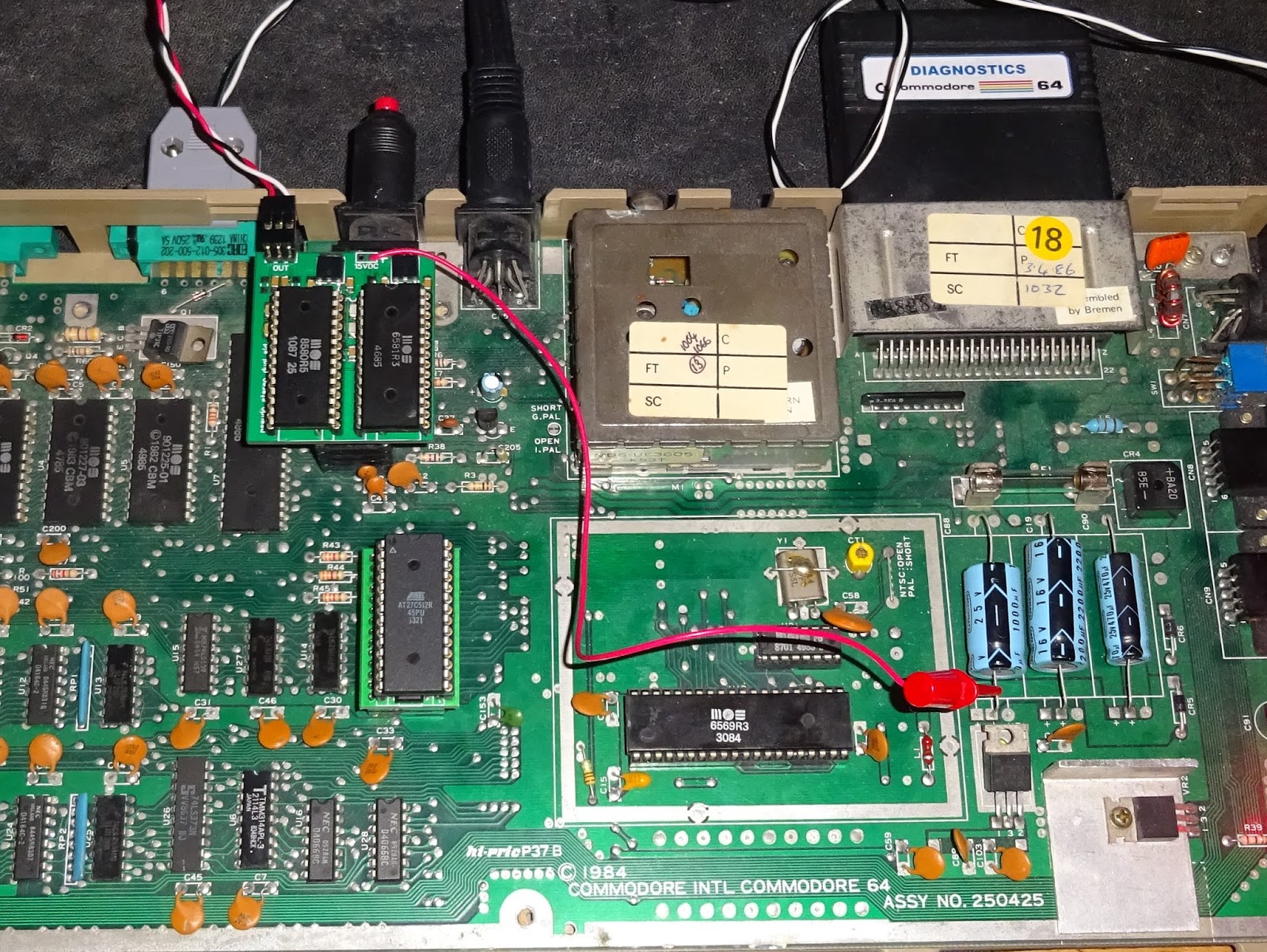
Second on the analogue side is the power supply. This is 12V for the older 6581 chip, and 9V for the later 8580. That confuses things a bit. The power is supplied from a 7812 regulator on the C64, and a zener diode / transistor regulator on the C64C. What I've done on these boards is ignore the supply voltage from the board, which may be 9V or 12V, and generate dedicated 9V or 12V rails for each chip with separate 78M09 and 78M12 regulators. The power for these comes from clipping onto the positive lead of reservoir capacitor C88 on the C64 board.
The C64C doesn't have that capactor easily accessible, but you can get a suitable supply by clipping onto the leg of CR3. All the chips I have tried draw around 60mA for a pair of SIDs, so this needs to be clipped onto anything that can supply 60mA at 15V-24V. When tapping power like this, it is always worth checking the voltages with a meter before using. It is also good to power up the system with the dual SID board installed and powered but no SID chips installed, and double check there is 12V on pin 28 of the 6581 socket and 9V on the 8580 socket.
Third on the analogue side are two filter capacitors for each chip. Different values are required for the 6581 and 8580, so again I ignore what is onboard and have individual capacitors for each chip. Some of the dual SID boards require you to clip off or change the ones onboard, but here I just don't connect to the onboard ones, so you can go back to a single SID if you want.
Finally comes the audio output. Here the output from SID 1 is fed through to the board as previously, so you get sound from the A/V port or TV output (is anyone still using TV output?). The outputs from both SIDs are also separately amplified and fed to a 3pin header for the stereo output. The audio output stages on the C64 and C64C were slightly different, the C64 had a capacitor bypassing the transistor from base to emitter, the C64C from emitter to ground. The board is laid out to take either arrangement, and I've been matching those to the chip, so the 6580 has the C64 version, 8581 has the C64C version. This further differentiates the stereo image.
SIDs are in short supply, and are used in various music gear outside the C64, so it is a bit luxurious to use two SIDs in one computer. However, you can use partly faulty SIDs here, I have one which locks up when you try to read from it, that is fine as SID2 here, as it will never be read. I also have a couple which have one or more voices missing. This makes the stereo a bit more varied, if a bit biased to one side or another.
The Psuedo stereo dual SID boards can be configured so each SID socket is setup for each a 6581 or 8580, independent on what was originally fitted to the Commdore 64. So you could even use this to fit a signle 6581 to a C64C or an 8580 to a C64, and leave the second socket empty.
As with the previous post on the C64 PLA replacements, the SID is in different locations depending on the revision of the board. In some cases, the rear connectors get in the way, so you may need to stack one or two sockets to raise it up to clear the socket. I'll address that on the next revision. There are also some capacitors around, just gently lean those out of the way, or again use riser sockets.
Keyboard clearance is sometimes tight, it varies with the model, the C64C is most difficult. A SwinSID may just fit, but the extra height is right on the edge. You may have to cut or remove the metallised cardboard cover.
I'm now off to listen to more game music in glorious (pseudo) stereo.
My old favourite Spellbound (by David Jones - not that one) has great music on the C64.
Any questions? See Commodore 64 Pseudo Stereo Dual SID Questions.

UPDATE:
There is now a new revision of this board. I have moved the second SID chip select to a jumper to the edge of the board so you can more easily wire this to one of the IO selects on the cart port, or even wire in a switch to have both options. That option is there on the previous version, but it's hidden under the chip.

UPDATE 2:
A couple of reviews:
ORDERING:
These are currently out of stock. If you are interested, see contact details above.

Friday 27 November 2015

Commodore 64 PLA replacements

This is an old post, preserved for reference.
The products and services mentioned within are no longer available.

A common cause of  a black screen*, garbage on the screen, intermittent startup or general instability in Commodore 64's is the 906114-01 PLA chip. A custom gate array chip which handles all the address decoding in the C64. As usual, original stocks dried up many years ago, but there are various options to replace these. It is sometimes a bit of a lottery, as the timing in the C64 was never quite right. You can get a C64 that will only work with some PLAs, or PLAs that will only work in certain C64s.
I've tried various things in the past, a popular option is to use an EPROM to replace the PLA. This just need a bit or rewiring, I've tried that a few times (see previous article on C64 EPROM PLA replacements). It sort of works, but with mixed results, better on some boards than others.
There are a few designs around using CPLDs, but most of the 5V ones have been discontinued, so they would need 3.3V to 5V level shifters  on the outputs. I did try building one with two GAL chips a couple of years ago. I'm going to revisit that at some point, as it should be viable, but I haven't quite got the equations right yet.
Timing seems to be an issue, only certain EPROMs seem to work at the right speed, the Atmel AT27C512R-45PU (45nS) being a good choice. It appears the reason for the timing issues is that one signal (/CASRAM) needs to be delayed a little longer than the rest. When designing the two GAL version above, I passed that signal from the first chip through to the second to get the additional delay. That led me to adding an additional gate delay onto the EPROM board. I built this one with TTL logic gates buffering the /CASRAM signal between the EPROM and the board, shown without the headers for clarity.
The jumpers select 1, 2, 3 or 4 gate propagation delays, adding around 30 to 120nS to that signal. That works well in a lot of cases, 1 or 2 delays (30nS or 60nS) seems to be good for a lot of boards. Another simple option demonstrated in this video shows you can get a similar effect by adding some additional capacitance to the pin.
I've built up some boards with space for a suitable capacitor, 68 or 82pF being around the right value. It should probably be an RC filter, but just the C seems to work.
I've tested this on several boards, and it seems to work quite well. Testing over several hours with the diagnostics cartridge and test harness and with an assortment of games it seems to run well,
I dug out a a couple of boards which has been a bit picky about PLAs in the past, one liked it, one didn't. I've used turned pin headers which fit into most sockets. I've had a few boards with intermittent sockets, so it is worth replacing them with turned pin sockets. Also in a fit of optimism, some boards actually have the PLA factory soldered in.
After all the above photos, this one may look like a mistake, I've put the PLA in the socket at the back of the case, not the middle. Bit it isn't a mistake, at least not a mistake by me. The PLA is indeed in a different place. For some reason Commodore had a board that had been around for several years and several revisions with the only two 28pin socketed chips close by each other in the middle of the board. When they came to revise that board, not much else changed (apart from the VIC II and surroundings). But some clever chap decided to swap around the SID and the PLA between the two most common versions of the C64, the 250407 and the 250425.
What's great is the SID has 12V on pin 28, and the PLA has 5V. Get them the wrong way around and you fry the PLA. If it doubt, power on with both sockets empty and measure the voltage at pin 28, or look for the two capacitors around pins 1-4 of the SID. I've had at least one C64 arrive with those chips the wrong way around, and a baking hot PLA running at 12V. Since the PLA outputs are pulled up to it's supply voltage, that also sends up to 12V to some of the pins that are outputs on the PLA. On the SID these pins are some of the data and address bus, so can send 12V to most of the chips on the board. Oh dear, not a good move.
I have some of both the logic gate delay and the capacitor delay board. I can supply these with a programmed 27C512, tested on some of my Commdore 64's.Whether they work on your particular C64 is difficult to say. It would be nice to have a guaranteed replacement, but no sign so far.

* N.B. when I say black screen, this is video sync but only a black screen displayed. This is different from no video sync, which usually indicates the VIC II chip is at fault.

Thursday 19 November 2015

VIC20 - The Penultimate Cartridge - Part 1

This is an old post, preserved for reference.
The products and services mentioned within are no longer available.

This is a quick preview of an upcoming project, in response to a video by GadgetUK164 on the VIC20, where he kindly mentioned my blog. I hope I haven't broken the internet with a circular reference.
This is a VIC20 cartridge I'm working on at the moment. In this version, it can provide the following features:
  • Selectable RAM upgrade, to to 32K
  • Selectable Read only for RAM blocks 3 and 5
  • Selectable ROM image, one of 8 - 8K ROM images only
  • Externally accessible configuration and reset switches
The memory can currently occupy the 3K expansion in block 0 (RAM1/2/3) and blocks 1,2,3 and 5. Block 5 is not counted by BASIC in the total, but can be used to load ROM images. This and block 3 can be made read only of cartridges that require that. I may remove the 3K option in future versions, unless anything specifically requires it. The selectable ROM images mean this can act as a real cartridge so you can have a selection of you favourite carts available at the flick of a switch (well, a couple of switches and a press of the reset button).
This fits into a standard cartridge case, with the DIP switch for configuration and a reset button sticking out. Most Commodore cartridge cases have the slot there, so I thought I'd use it to add the external switches, so no drilling or cutting of the case is required.
Inside, there is a 32K RAM chip and currently, a 512K EPROM, although I'll be putting a large ROM in later versions. The smaller chip is a GAL which handles the address decoding.
There is a lot of space left on the board, deliberately. This space will be used to add the following features:
  • Selectable ROM image, one of 32 up to 16K ROM images
  • Integrated IEEE-488 adapter
  • Integrated IEEE-488 SD card disk drive (a version of PET microSD)
This should result in a self contained cartridge with just the configuration switches, reset button, activity LEDs and microSD card sticking out. No additional wires for power or the IEC port, it will all be contained within the cartridge. The parallel IEEE-488 bus is also a lot faster than the serial IEC bus, so there should be a speed improvement as well. I have previously tested that the PET microSD on a VIC20, and it works well.
More revision of that to come, on the way to 'the Penultimate Cartridge'. I've decided to call it that as every time there is a Final or Ultimate cartridges there seem to be quite a lot of versions that follow it. So I thought I'd be honest with the name on this one.

Update:
There is now a V2 board, with the additional option of 3K + 8K + 8K + 8K + 8K to give 35K which only seems to be used by the VIC20 port of DOOM. The V2 boards can also support up to 32 x 16K cartridges, see the article on the VIC20 Penultimate Cartridge V2 for more info.


On a slightly related note, the issues in GadgetUK164's video with Rockwell chips, I can't say I've had any problems. I've tested this on a VIC20 with a Rockwell R6522P, and they are fine, as expected. Also tested with the original CPU (a standard MOS 6502) and a Rockwell R6502P. I've used this to load Dig Dug from an SD2IEC into my Penultimate Cartridge, and that seems to run fine with no need for the diode mod. Maybe he had a duff chip, or a fault elsewhere on that particular VIC20.
As far as I know, it's only the WDC W65C22S chips which changed the IRQ pin (to improve speed). They also produce a W65C22N version, which is compatible with the older NMOS devices (like the R6522P and the MOS 6522), and that also works fine in the VIC20.
It's good to know you can buy modern replacement parts without having to risk 'new old stock' from China.  I've used these in VIC20s, PETs, BBC etc. I also use a lot of W65C21N (again the N suffix is important for NMOS compatibility). This is a replacement for 6520, 6521, 6821 etc. and I've used those in PETs, Dragon32's, Atari 800XL etc.
So I had no problems loading or running Dig Dug with Rockwell chips or WDC chips (or Synertek for that matter).

Update: As requested, I've also checked the Rockwell R6522AP, which is just their version of the MOS 6522A, which is a faster speed graded version of the MOS 6522.

2022 Update: The production version of the Penultimate Cartridge is now available from  The Future Was 8 bit

Saturday 7 November 2015

Commodore PET 2001-8 Mainboard Repair - Part 2

This is an old post, preserved for reference.
The products and services mentioned within are no longer available.

Part 1 of this Commodore PET 2001-8 repair left the main board running, but with most of the parts replaced.
In that state it's all working, so now I can put back any of original parts which are working. I used the ROM/RAM board to identify the faulty ROM and RAM chips. The latest version allows me to test individual ROMs (or pairs or ROMs). From this, four of the seven ROMs were bad.
To test the RAM chips, I used the PET tester ROM image which tests the first 1K of RAM. By shuffling the 6550s into the right most sockets, I was able to find a pair that worked. I can then test all the chips using one good one and one potentially bad one at a time.
This is a typical result, G shows a good bit, B a bad one. If you look carefully, you can see a couple of bits of memory that actually work. Fourteen of the eighteen chips were bad. I did manage to get it to work as a 2K machine.
But that's not much use as there is just under 1K available to use. Fine if you are a ZX81, but not much use here. Notice the old character ROM is still in there - 1023 BYTES FREE. This was before that new character ROM was installed.
There are replacements for the 6550s available, each using a single 2114 chip, but replacing all of those would work out rather expensive. Given that four of the ROMs were also bad, we've gone for the option of leaving the ROM/RAM board in place. This comes with the option of running with BASIC 2 and 8K of RAM as it originally was, or selecting from 8K, 16K or 32K RAM and BASIC 1,2 or 4, so you can have the fully loaded 32K and BASIC 4. I was, however, able to use two of the working 6550 RAM chips from main RAM to replace the video RAM.
The CPU and keyboard VIA were confirmed as faulty, the other VIA was just bad contacts. The PIA was also fine after the edge connectors were cleaned. One datasette was still not working. I noticed the central leg on one of the TIP 29 transistors was actually snapped. I've unclipped the heatsink to show it more clearly.
These transistors are 'flapping about in the breeze' with clip on heatsinks, and so prone to stress the legs. One looked to have been replaced in the past, but I replaced both anyway as it looked like it that could be starting to go as well. These control the motors in the datasettes, and they are now both working. Later PET boards had these riveted to the boards, with no heatsinks. Later still, on things like the Commodore 64, the transistors were back to levitating above the board.
The two bypass capacitors on the main rectifier diodes were also down a leg each, so I replaced those.
The originals were rather large 10nF ceramic capacitors, so I replaced those with 10nF axial ceramic capacitors so it wouldn't happen again. It would work (and obviously had been working) fine without them, they just reduce the RF noise a bit.
This also shows the replacement power socket. This is a new one as the original had wires soldered onto it. To go with that, I made up a new wiring harness, but have also supplied a short lead with just with 5 wires, in case the owner prefers to avoid soldering to the transformer and keeps the terminal block.
With everything back together, I can get back to testing. The original 2001 has a built in diagnostic, activated by a special loopback plug on the user port.
When that is running. a small square moves over each position on the screen, then it shows the character map and lights the red LED on the board if all is well.  You can just see the LED in the centre of this photo, artistically framed by the keyboard loopback plug.
Not that useful really, later PETs replaced this with the machine code monitor - which is why the monitor is sometimes activated when you have problems with the 6522 VIA that monitors the diagnostic pin. At least you can see the problem with the character ROM has been fixed.
The owner had requested a PET microSD to go with their newly repaired PET. I initially had problems with the IEEE-488 on this PET, testing with my IEEE-488 diagnostic board showed up intermittent connections on the edge connector, but after a good clean, it was fine.
Don't worry, I won't be sending it back with all those boards hanging out the back, I'll be using the internal version of the PET microSD, to keep it all self contained and tidy.
That normally gets it's power from the internal power connector which is fitted on most later PETs. The 2001 doesn't have that, so for these. I supply a longer lead with a clip on the end to attach to the unregulated 9V supply, right where it enters the board on the reverse protection diode.
This should minimise the impact of the PET microSD on the power supply. The original board would have drawn between 3 and 4amps on the 9v rail. With the ROM/RAM board, this is now about 1 amp. With the PET microSD, it's around 1.1 amps.
Here is the final repaired board, ready to go back.
The main issues:
  • Faulty ROM and RAM - replaced by ROM/RAM board
  • Faulty CPU - replaced with NOS 6502
  • Faulty keyboard VIA - replaced by WDC 65C21N
  • Damaged TIP29s - replaced by NOS TIP29
  • Partly faulty character ROM - replaced by 2716 EPROM and adapter
  • Faulty video RAM - replaced by 6550s from main RAM
  • Soldered on power cable - replaced by plug and socket and new wiring harness
That's has been run in with various tests and seems very stable. The only real issue being the noise on the screen when updating fast which is inherent in the design of the 2001.
The result of all of this? - my Tetris score is getting better....