
I have been expanding the instruction manual for my Minstrel ZX80 Clone to include more information on how the ZX80 works. I thought it would be good to expand on that even more here. So, how does the ZX80 work?

The Sinclair ZX80 is a low cost home computer, launched in 1980 with a price tag of £99, considerably cheaper than it's contemporary counterparts. How did they do that? Well, the first thing to know about the ZX80 is that it's main job is not to run your code. That's very much a side task. The thing it spends most of it's time doing is drawing a picture on the TV screen. And it does that by executing mainly NOP instructions.

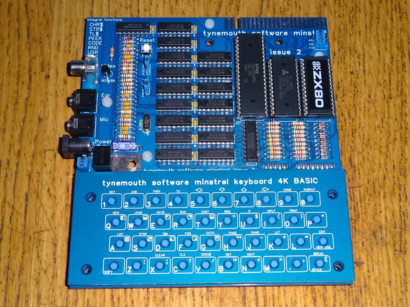
Unlike most other computers of it's era, it doesn't have a video chip. It doesn't have any custom chips in fact. There is a Z80 CPU, a 4K ROM chip, two 1K x 4 bit static RAM chips, and seventeen 74 series TTL chips, and that's it.

Quite an achievement to make a functional computer out of that, and how it does it is very clever, and I hope to try an explain that here. I am using schematics, screenshots and logic plots from my Minstrel ZX80 clones. These follow the same design, using the same chips, and the only modern substitutions being more easily available ROM and RAM chips, and an extra TTL chip to bring the composite video closer to that required by most modern TV sets.

Oh, and I do have better keyboards available, but you can go back to a membrane if you wish.
The Z80

Well, first off, the heart of the system is the Z80 processor. This has been in continuous production since 1976, and is still going strong. Here a Z80 or Z80A is clocked at 3.25MHz (yes, more than three times faster than the 6502 in the PET, VIC20 and even the C64), although in practice, the Z80 takes more cycles per instruction that the 6502, so there's not much in it. The /Halt, /NMI and /BusRequest control inputs to the Z80 are pulled high, leaving them in a stable state and able to be driven low to activate them. A minimal reset circuit is used, consisting of a resistor and capacitor. This holds the reset line low for around 100mS until the 1uF capacitor has charged to past the logic low level.
The Edge Connector

The ZX80 expansion edge connector is connected pretty much directly to the Z80. This exposes most of the pins of the Z80 to allow expansion to the system. It also includes power for peripherals, and a way to disable the onboard RAM. The ZX81 that followed used the same edge connector, other than a spare pin was used to also allow you to disable the onboard ROM. That has been implemented on the Minstrel ZX80 clone in the same way as the ZX81.
RAM

The ZX80 originally came with 1K of static RAM as two 2114 SRAM chips. Unlike the Z80 and all the TTL chips, the small SRAM chips are out of production. However larger modern RAM chips are available which can be addressed in the same way. In the Minstrel ZX80 clone, a 32K RAM chip has been used, as that is the most easily available (8K chips are available but are often more expensive than the 32K versions). The address decoding is identical, and is fairly minimal. If A14 is high, and the Z80 is performing a memory request, the RAM is enabled. Resistor R19 is connected between the two chips to allow the chip select signal at the chip side to be connected to the edge connector. Pulling this high will disable the internal RAM and allow an external peripheral to replace the RAM. This happened in the ZX80 and ZX81 when a 16K RAM pack was fitted, the internal 1K of RAM was disabled (a bit wasteful given the price of RAM in those days). The initial offering for the ZX80 was a 3K expansion that used another six 2114 chips to take the RAM to 4K. Using A14 as the only decoding means the RAM is present at address 4000-7FFF and mirrored at C000-FFFF. Originally the 1K would have also been mirrored 16 times within each of those blocks, but here the full 16K block is used as RAM. The RAM chip is a 32K chip, but has the highest address line tied high, so half of the chip is not used. Due to the way the RAM is used, it would have required additional decoding logic to add the other 16K, so it is not used to maintain compatibility, and very little software would had used it.
ROM

The original ZX80 came with a 4K ROM chip. The chip select line was activated when there was a memory request and A14 was low. That meant the ROM chip was enabled from 0000-3FFF and duplicated at 8000-BFFF, and the 4K chip is mirrored 4 times in each 16K block. The ZX80 could be upgraded to ZX81 style BASIC, which came in an 8K ROM. The Minstrel ZX80 clone uses a larger EPROM, a 27C64 up to a 27C512, with multiple 8K chunks selectable via jumpers so you can have a choice of ROM versions.
Memory Map
The following table shows the memory map for four machines. An original ZX80; a ZX80 which has been upgraded with the 8K BASIC ROM and a 3K RAM pack (giving 4K in total); a ZX80 that has been upgraded with the 8K BASIC and a 16K RAM pack; and finally, the Minstrel ZX80 clone.
Address Range |
Original ZX80 |
Upgraded ZX80 |
ZX80 + 16K RAM |
Minstrel ZX80 Clone |
0000-0FFF |
4K ROM |
8K ROM |
8K ROM |
8K ROM |
1000-1FFF |
4K ROM* |
|||
2000-2FFF |
4K ROM* |
8K ROM* |
8K ROM* |
8K ROM* |
3000-3FFF |
4K ROM* |
|||
4000-4FFF |
1K RAM x4 |
4K RAM |
16K RAM |
16K RAM |
5000-5FFF |
1K RAM x4* |
4K RAM* |
||
6000-6FFF |
1K RAM x4* |
4K RAM* |
||
7000-7FFF |
1K RAM x4* |
4K RAM* |
||
8000-8FFF |
4K ROM# |
8K ROM# |
8K ROM# |
8K ROM# |
9000-9FFF |
4K ROM# |
|||
A000-AFFF |
4K ROM# |
8K ROM# |
8K ROM# |
8K ROM# |
B000-BFFF |
4K ROM# |
|||
C000-CFFF |
1K RAM x4# |
4K RAM# |
16K RAM# |
16K RAM# |
D000-DFFF |
1K RAM x4# |
4K RAM# |
||
E000-EFFF |
1K RAM x4# |
4K RAM# |
||
F000-FFFF |
1K RAM x4# |
4K RAM# |
* Mirrored copy # Mirrored copy used for display generation
Operating States
You may have noticed the address and data lines on the ROM and RAM chip are not simply labelled D0-D7 and A0-A15. Due to the way the ZX80 is run, there are two versions of the databus and two versions of the address bus. OK, buckle in, this is where it gets unusual.
The screen information is stored in RAM, and the ZX80 uses the way it is mirrored at the top of the address range to trigger the screen drawing hardware. It tries to execute the high mirror of the screen information (called the display file or DFILE), and this is intercepted by hardware, to trick the processor into executing a NOP or 'no operation instruction' and then step up to the next character in the display file and so on until the screen has completed. It does this in real time, generating the video output signal as it goes, when it gets to the bottom of the screen, it has a brief period where it checks to see if a key has been pressed. If not, it goes back to the top and is just in time to start drawing the next frame of the video signal. Fifty times a second, to match the 50Hz frame rate of PAL (or 60 times a second for NTSC).
If a key is pressed, it can't do anything about that and draw the screen at the same time, so it goes away to process the key press, and whilst it is doing that, the screen does not get drawn, no video is generated. When it is finished processing the key press, it goes back to drawing the screen. This generates the characteristic flashing on the screen every time you press a key. If you ask it to do something more complicated, whilst it is doing that. the screen will be off for as long as it takes, and will only be drawn again when it is finished.

The ZX81 got around this by running code in the period between the bottom one one frame of video and the top of the next, but that needed extra hardware. It is possible to do this on the ZX80 in certain circumstances, and there is an art to writing 'Flicker Free' games, when requires code to be of a fixed number of cycles exactly equalling the period between frames. More information about this (and a selection of Flicker Free Games can be found on Paul Farrow's Page).
Clock

The ZX80 clock runs at 6.5MHz, and so each clock pulse lasts 0.15uS. The standard PAL video scan line is 64uS long. The ZX80 has 32 character lines, 8 pixels per character, so each clock pulse has to generate a single pixel. That takes up just under 40uS for the section of the screen with characters on, with a synchronisation pulse at the start and blank areas either side of the characters. That is 8 clock pulses per character. The Z80 is clocked at half that speed, so each character is four Z80 clock cycles, which is how long the Z80 takes to execute a single NOP instruction. How on Earth does it do it?

The main clock is divided by two by a 74LS74 D type flip flop, which generates 3.25MHz clocks in inverted and non-inverted format, and also a buffered version driven by two open collector inverters to give a good clean fast clock pulse for the Z80. The NOP instruction takes four cycles, and during this time, the Z80 goes through several states, labelled T1 through T4. Some instruction take a different numbers of cycles, some require additional reads to complete multipart instructions, some take longer to process etc. I'll concentrate on NOP as that is the main instruction that the Z80 in a ZX80 executes. During the first two cycles, the opcode is read from memory, and during the next two, cycles it is executed.
State |
Address Bus |
Data Bus |
T1 |
PC (code address) |
- |
T2 |
PC (code address) |
Op code |
T3 |
- |
- |
T4 |
- |
- |
The Program Counter (PC) is sent to the address bus at the start of the first cycle, and the memory device that is providing the data is expected to have set the databus appropriately by the start of the second cycle. The third and forth cycles don't need to use either the address or data busses, so they could just sit idle.
The Z80 has a neat feature designed to work with dynamic RAM. DRAM (i.e. the good old 4116 chip) was much cheaper that static RAM (i.e. the 2114 used in the ZX80 or the 65526 used in the Minstrel). However, DRAM had a failing, that it is a very short term memory. The memory needs to be 'refreshed' by repeatedly accessing each bit of memory many times every second. Normally that means the system designers would have to setup a separate counter to clock through each of the addresses, and switch to that when the RAM wasn't being used by the CPU. The Z80 thoughtfully provides a refresh signal that is asserted whenever the processor is busy doing something for a few clock cycles. A separate 'R' address register steps through to the next address each time it is used, so the refreshing can be carried out as a background task. With the NOP instruction, the T3 and T4 states are used to refresh DRAM. Data is returned from the refresh operation, but it is ignored by the processor.
State |
Address Bus |
Data Bus |
T1 |
PC (code address) |
- |
T2 |
PC (code address) |
Op code |
T3 |
R (refresh address) |
- |
T4 |
R (refresh address) |
refresh data (ignored) |
The designers of the ZX80 somewhat subverted this process. When an opcode read is detected for an address over the 32K boundary (i.e. the display file), the databus is split, and the Z80 is fed the opcode for a NOP operation (which is 0x00), whilst the actual value read is the next character to be displayed on the screen.

The split is archived by eight resistors. The Z80, NOP generator (see below) and the IO chip (later) sit on the CPU side. On the other side, the alternative databus, sits the ROM, the RAM and the external bus. This is labelled as Alt_D0-7, although it was shown on the original schematics, as D0'-D7'. I have not used that terminology as it can be difficult to see sometimes.
NOP Generator

The NOP instruction is 0x00, and this is forced on the CPU side of the databus using eight 74LS05 open collector inverters, so when their inputs are high, they drive the bus low. The logic which generates it also requires that the alternate D6 is low, and the /Halt line is high, as these are used to stop the process. OK, so we are two cycles in, and we have a character code, for example 0xB0, which is an inverse K (since that is the first thing which is displayed on the screen). To turn that into pixels, we need a character ROM. That's easy, that just sits at the end of the main system ROM. We also need to know which line we are drawing, as each character is eight pixels wide, eight pixels high, and so it takes 8 lines on the TV to display a row of characters.

Here we have some decoding logic which basically says 'latch what is on the databus when refresh is high, the clock is high, and MREQ is low). This happens at the end of the T1 and T2 states. Whatever is read at the end of T1 is ignored and overwritten at the end of the T2 state. The 74LS373 latch stores the character code we read from the RAM before. The 74LS393 is a counter which is incremented every line, and reset at the top of the screen. This gives the lower three bits of the character address. The next six come from the character code, and the rest is made up from the refresh address the Z80 generates, which is adjusted to point to the character table at the end of the ROM.

The address bus for the ROM chip is multiplexed using three 74LS157 quad mux chips. These are controlled by the refresh line, which is high during the T1 and T2 states (where the ROM chip is attached to the CPU address bus), and low during the T3 and T4 states (where the ROM is addressed by the address made up of the line counter, the character code and the ROM address from top bits of the processor refresh address). That uses nine of the twelve mux switches. One more is used to enable the ROM chip during the Refresh cycle by switching the ROM_CS line low. The final two muxes buffer the A14 and A15 address lines. This add a small delay to the higher address lines, which without them can cause a glitch on the shift/load line.
State |
Z80 Address Bus |
Z80 Data Bus |
Alt Data Bus |
Alt Address Bus |
T1 |
PC (DFILE address) |
- |
PC (DFILE address) |
Previous Character Data |
T2 |
PC (DFILE address) |
NOP |
PC (DFILE address) |
- |
T3 |
R (refresh address) |
- |
Character Address |
- |
T4 |
R (refresh address) |
- |
Character Address |
New Character Data |
At the start of the T1 cycle, the databus still contains the character pixel data previously read from the ROM. This is clocked into the shift register and then clocked out with eight 6.5MHz clock pulses, just in time for the next character to be ready.
This shows two character reads here the fifth line of characters 0 and inverse L. The seventh bit of character data is a signal to invert the character (white on black instead of black on white). Here the second cycle clocks out a row of the inverted 'L' character, so you can see the character lines up with the next four cycles.

The 'invert this character' signal is stored in a separate latch, cleared at the start of the next T1 state. Note the character pixels aren't synchronised with the clock and the right hand pixel is a little thinner than the rest due to the way the pulses are timed.

This character generation goes on until the end of the line is reached. This is signalled by a Halt instruction (0x76) being read. This has bit 6 set, so the NOP generator is disabled, and the Z80 reads and executes the halt instruction and the Z80 is halted. The clock keeps running, and the Z80 executes NOP instructions (generated internally this time, the NOP generator is not active). The refresh cycles continue, and at the end of the line, the refresh counter has reached a point where the A6 part of the address (which was high at the start) goes low. A6 is hard wired to the interrupt pin on the Z80, so it causes an interrupt, and the Z80 fires up again and get sready for the next line. It runs through the same sequence eight times for each row of characters, then steps to the next row. When it runs out of lines to draw, it stops (this is handled by the code in ROM).

Responding to the interrupt generated by A6 going low causes an INTACK signal (M1 and IORQ are low at the same time). This presets the left hand of the three D type flip flops used to generate the sync signals. This is then clocked through on subsequent cycles using the M1 pulse which is low during the T1 and T2 states when it is reading an Opcode. Here it is inverted to clock the flip flops which together generate a Sync pulse which is 20 cycles long (6.15uS), this is a little longer that the specified 4.7uS of a horizontal sync pulse, but close enough.

On the original ZX80 (and early ZX81s), the video output then went high, to the white level, and dropped down to black when characters were present. This was fine with older TV sets, but caused problems for modern LCD TVs. Later versions of the ZX81 added the missing 'backporch' signal which sets the black level after the sync pulse, before going to the white level. This is achieved on the Minstrel by stretching the sync pulse and holding the video low during this period. (see an old blog post where this was added to the first versions of the Minstrel - Minstrel ZX80 Clone Video Output Enhancement).

The Minstrel also added the transistor buffer to give a stronger composite video output, which is generated by combing the Sync signal with the video signal. The optional resistor R100 reduces the video level for some TV SCART inputs.
Input / Output
At the end of the screen, a vertical sync pulse is required, this is controlled by a flip flop set by read operations, and cleared by write operations. It uses minimally decoded output ports to achieve this.

Any IO write will clear the VSync flip flop, and a read to any even address will set /VSync again. This decoding wastes almost half of the available input addresses, but saves several logic chips required to decode that with greater specificity. That read address is used for an input buffer which is a 74LS365 hex buffer, with 5 inputs which are the keyboard sense lines, and one which is the input from the cassette port. When active, these can be read on the CPU side of the databus.

An extra bit of IO is achieved using Diode D11. When the NTSC link is fitted, this pulls D6 low when the keyboard is read, and is used to decided on 50Hz or 60Hz video frames.

The keyboard is made up of 40 keys arranged as an 8x5 matrix, shown above on the PCB of my Minstrel tact switch keyboard. The original was created using a circular pattern of interspersed row and column wires at each cross point in the matrix. The key was 'pressed' by a foil pad on the underside of the keyboard overlay pressing shorting the two rings together. (shown here on a 1980s ZX80 clone, the Micro Ace I repaired a few years ago).

The keyboard rows are driven by diodes from the high 8 bits of the address bus, so by using a 16 bit input instruction, you can select which rows to read from.

When an address line is low, and a key is pressed, the relevant column input reads low. Reading the input port with an address with a high byte of all zeroes with indicate if any keys are pressed anywhere on the matrix, and so it is worth scanning individually.
Cassette IO
Finally, the main source of file loading and saving is does with a normal audio cassette recorder. Two 3.5mm mono jacks provide Mic (output) and Ear (input) input connections. These ports include a bit of filtering, but it often took quite a bit of fiddling with volume and tone controls to get a valid signal out of the tape.

The video sync signal is used to drive the Mic, the low pass filter removes the 15KHz HSync pulses and leaves the VSync pulses which are set by the flip flops. When data is being loaded or saved, the screen display is disabled (remember the ZX80 can only do the screen drawing thing when it isn't doing anything else). When this is going on, the data can be seen on the screen as a patterns of lines. An experienced user can tell when things are going right, although modern TVs normally shut off at this point.

Abbreviated display files
Just in case anyone was still reading (and possibly even following) this, there is a bit I missed out above. In the original ZX80 4K BASIC ROM, the display file works slightly differently, it is abbreviated to use a minimal amount of RAM. It is also abbreviated on the upgrade 8K BASIC ROM when there is less than 4K of RAM installed. Rather than storing 24 lines of 32 characters, it stores 24 lines of 'up to 32 characters'. Each one starts and ends with the Halt instruction, but if there are no characters on that line, the end Halt follows directly on from the first one, saving 32 bytes per line. Considering 24 x (32+1+1) is 816 bytes and the ZX80 only had 1024 bytes in total, you can see why it was useful to reduce the size where possible.

This shows the output from a specially modified ZX80. Here I have fed a checkerboard pattern into the serial input of the 74LS165 shift register. If no parallel data is applied to it (i.e. if there is no character in the DFILE), it will defer to the serial input. Normally, the serial input is connected to 0V, so it appears like a space character. Here I have connected this to the 3.25MHz clock XORed with the lowest bit of the line counter so it generates a dot pattern which alternates each line.

I have typed in a short program, and you can see the lines are only filled where there are characters to display, and then as soon as the end of a run of characters is reached, the data stops and the Z80 would be halted until the end of the screen line.

The program prints out lines of Xs of a random length. Again you can see the DFILE will only be half the size it would have been if it wasn't abbreviated.

On the 8K ROM version of BASIC, when there is 4K or more RAM installed, you can see the full screen is filled with space characters before it starts. I think it is a combination of the extra RAM checks and filling up the DFILE that results in systems with 4K or more RAM taking a little longer before the K appears after power on.

With the full DFILE, the listing has space all around. Also note that with the upgraded version of BASIC, the syntax of the RND command is different, as is the font, with narrower characters and a slashed zero.

If I zoom into one of those screens, you can see the dots in the greyscale section. The grey border is sort of growing on me, I might look at making it an option on the next version of the Minstrel?

Each dot is one 6.5MHz clock pulse. Each adjacent pair of black and white dots is one 3.25MHz clock pulse. Each line of 8 black and white dots is a single NOP instruction. And within the time it takes to read and execute that single instruction, the dot pattern of a character is generated. It's amazing really.

The line generation is the same for PAL and NTSC. The 64uS lines are close enough to the requirements for both standards. The same number of characters are generated, the only difference being the shorter section at the top and bottom of the screen to make 60 frames every second rather than 50.

The mode is read from the PAL/NTSC jumper each frame, so you can change it on the fly as the machine is running. After all, why read it once and store it in memory, wasting a precious byte, when you can read it from hardware each frame.

Amazing really, a 24x32 character display composite video system built from TTL chips and ingenuity.
Build your own
So that's about it for the ZX80. Now you know how it works, you can build you own. All you need is this collection of bits available from my Tindie store.

Once you put that all together, you can add a keyboard and away you go.

As ever, with ZX80 stuff, I have to thank Grant Searle for his excellent website on the ZX80 and other 8 bit machines.
Adverts
The Minstrel 2, 3 and recently relaunched Minstrel 4th are available on my Tindie store.
- https://www.tindie.com/products/tynemouth/minstrel-2-with-keyboard-z80-based-zx80-kit/
- https://www.tindie.com/products/tynemouth/minstrel-3-with-keyboard-z80-based-zx81-kit/
- https://www.tindie.com/products/tynemouth/minstrel-4th-z80-forth-rc2014-jupiter-ace-kit/
The Minstrel 4th now features multiple ROM images, so you can run Forth or ZX80 or ZX81 BASIC, including slow mode. The BASICs are still experimental. They are fairly compatible, most things work, with a few caveats if programs have their own video routines for pseudo-high-resolution graphics modes or fancy loaders etc.

Yes, you can run 3D Monster Maze - that was my target. This is the original unmodified version, loaded from tape.
Patreon
You can support me via Patreon, and get access to advance previews of development logs on new projects and behind the scenes updates. New releases like this will be notified to Patreon first, if you want to be sure to get the latest things. This also includes access to my Patreon only Discord server for even more regular updates.
